Semiconductor device having an Anti-pad peeling-off structure
Inactive Publication Date: 2010-01-07
SAMSUNG ELECTRONICS CO LTD
View PDF0 Cites 6 Cited by
Summary
Abstract
Description
Claims
Application Information
AI Technical Summary
This helps you quickly interpret patents by identifying the three key elements:
Problems solved by technology
Method used
Benefits of technology
Benefits of technology
[0011]Example embodiments of the present invention provide a semiconductor device having an anti-pad peeling-off structure capable of overcoming stresses applied to a metal pad during a bonding process.
[0017]According to an aspect of the present invention, a plurality of the slits is formed in the metal pad layer and the protecting layer is formed on the slits, thereby preventing peeling-off of the metal pad layer.
[0018]The structure under the metal pad may have a concavo-convex structure capable of increasing adhesive strength with a lower surface of the metal pad layer, thereby preventing peeling-off of the metal pad layer.
[0019]Since the residual protecting layer pattern in the slits of the metal pad layer includes a material different from the metal pad layer, the residual protecting layer pattern may provide a buffer when physical impacts are generated or may terminate cracks generated in the metal pad.
[0020]Moreover, the protruding shape of the protecting layer pattern may overcome pull-back stresses during a wire bonding process, thereby preventing peeling-off of the metal pad layer.
Problems solved by technology
When physical or electrical impacts occur in the unit cell, the impacts may not be buffered or distributed due to the reduced dimensions of the unit cell so that failures occur frequently in the device.
If the physical stresses are not absorbed or distributed, adhesion strength between the metal pad and an underlying layer thereof is decreased, which may cause the metal pad to peel off from the underlying layer.
Accordingly, disconnection problems between the semiconductor device and an external system are generated by peeling-off of the metal pad.
Method used
Image
Click on the blue label to locate the original text in one second.
Reading with bidirectional positioning of images and text.
Examples
embodiment 1
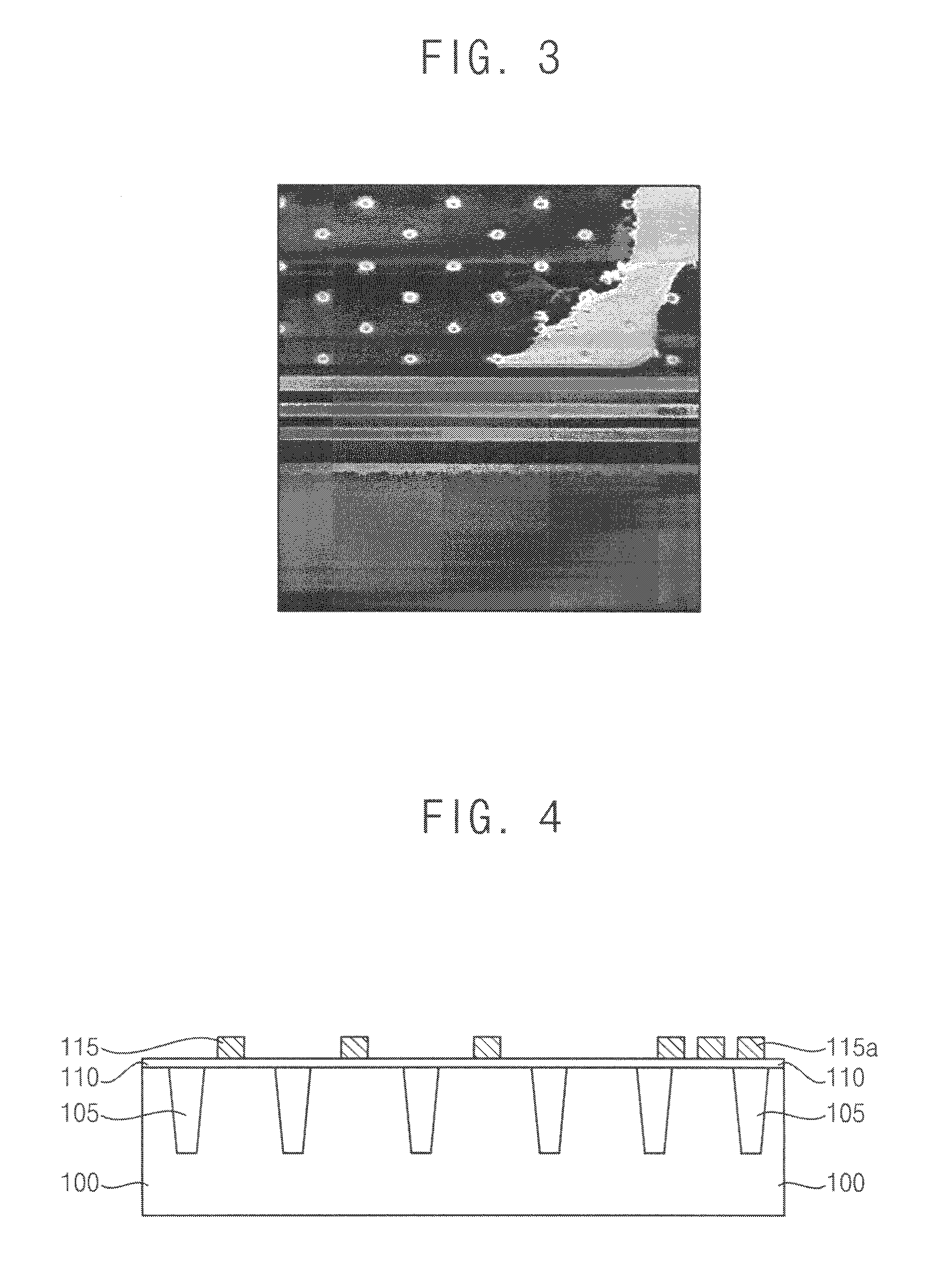
[0035]FIGS. 4 to 9 are cross-sectional views illustrating a method of manufacturing a semiconductor device having an anti-pad peeling-off structure in accordance with a first example embodiment.
[0036]Referring to FIG. 4, a semiconductor device according to a first example embodiment is divided into a region for elements to be formed and a region for pads to be formed. The pads may be formed in a peripheral region of the semiconductor device. Alternatively, the pads may be formed in the central region according to an arrangement of pins in a packaging process.
[0037]Hereinafter, a method of manufacturing a semiconductor device including pads formed in a right peripheral region will explained for clarity.
[0071]FIGS. 13 to 19 are cross-sectional views illustrating a method of manufacturing a semiconductor device having an anti-pad peeling-off structure in accordance with a second exemplary embodiment.
[0072]Referring to FIG. 13, a semiconductor device according to a second exemplary embodiment is divided into a region for elements to be formed and a region for pads to be formed. The pads may be formed in a peripheral region of the semiconductor device. Alternatively, the pads may be formed in the central region according to an arrangement of pins in a packaging process.
[0073]Hereinafter, a method of manufacturing a semiconductor device including pads formed in a right peripheral region will be explained for clarity.
[0074]An isolation layer 205 is formed in a semiconductor substrate 200. The isolation layer 205 may be formed by a STI process or a LOCOS process.
[0075]After forming the isolation layer 205, a gate dielectric layer 210 is formed on the semiconductor substrate 200. The semi...
embodiment 3
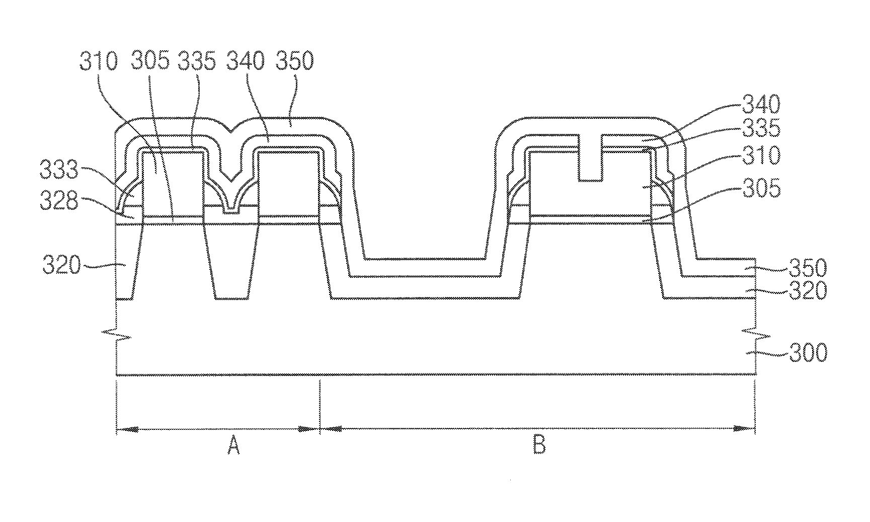
[0103]FIGS. 20 to 39 are cross-sectional views illustrating a method of manufacturing a flash memory device having an anti-pad peeling-off structure in accordance with a third exemplary embodiment.
[0104]Referring to FIG. 20, in a method of forming a flash memory device according to a third exemplary embodiment, a tunnel oxide layer 305, an electrode layer 310 and a hard mask layer 315 are sequentially formed on a substrate 300. The substrate 300 may include a siliconwafer or a SOI substrate.
[0105]In this embodiment, the substrate may be divided into a region A for memory cells to be formed and a region B for peripheral circuits such as high voltage transistors to be formed. Slits may be formed on the peripheral region B.
[0106]The tunnel oxide layer 305 may be formed to have a thickness of 50 Å to 100 Å by a thermal oxidation process. The tunnel oxide layer 305 may be formed using a material having excellent film characteristics for reading / writing operations of the device. Accordin...
PUM
Abstract
A bonding pad having an anti-pad peeling-off structure is disclosed. In a method of forming the bonding pad, after a metal pad layer is formed, a slit is formed in the metal pad layer. A protecting layer is formed on the metal pad layer. The protecting layer is partially removed to expose the metal pad such that a portion of the protecting layer remains in the slits to be connected to the main protecting layer. The protecting layer formed in the slit is connected to the protecting layer such that the residual protecting layer pattern buffer when physical impacts are generated, to prevent peeling-off of the metal pad layer.
Description
CROSS-REFERENCE TO RELATED PATENT APPLICATION[0001]This application claims priority under 35 U.S.C. § 119 from Korean Patent Application No. 10-2008-0065410, filed on Jul. 7, 2008 in the Korean Intellectual Property Office, the contents of which are herein incorporated by reference in their entirety.BACKGROUND[0002]1. Field of the Invention[0003]Methods and apparatuses consistent with exemplary embodiments of the present invention relate to a semiconductor device having an anti-pad peeling-off structure and a method of manufacturing the same. More particularly, example embodiments relate to a semiconductor device having an anti-pad peeling-off structure capable of overcoming stresses applied to a metal pad during a bonding process and a method of manufacturing the same.[0004]2. Description of the Related Art[0005]Generally, as semiconductor devices become highly integrated, dimensions of cells are reduced. Accordingly, it may be important to ensure physical and electrical properties...
Claims
Application Information
Patent Timeline
Application Date:The date an application was filed.
Publication Date:The date a patent or application was officially published.
First Publication Date:The earliest publication date of a patent with the same application number.
Issue Date:Publication date of the patent grant document.
PCT Entry Date:The Entry date of PCT National Phase.
Estimated Expiry Date:The statutory expiry date of a patent right according to the Patent Law, and it is the longest term of protection that the patent right can achieve without the termination of the patent right due to other reasons(Term extension factor has been taken into account ).
Invalid Date:Actual expiry date is based on effective date or publication date of legal transaction data of invalid patent.

