
High voltage device and method of fabricating the same

a high-voltage device and fabrication method technology, applied in semiconductor devices, semiconductor/solid-state device details, electrical apparatus, etc., can solve the problems of affecting the thickness of the resulting silicon oxide layer becomes non-uniform, and the thin gate oxide layer easily induces a breakdown, so as to mitigate the time-dependent dielectric breakdown characteristic and improve the reliability of the device

Active Publication Date: 2009-03-12
UNITED MICROELECTRONICS CORP
View PDF10 Cites 2 Cited by
  • Summary
  • Abstract
  • Description
  • Claims
  • Application Information

AI Technical Summary

Benefits of technology

[0006]The present invention is to provide a high voltage device and a method of fabricating the same, wherein the gate dielectric layer of the high voltage device has a uniform thickness for mitigating the time-dependent dielectric breakdown characteristic and for improving the reliability of the device.
[0034]According to an embodiment of the method of fabricating a high voltage device of the present invention, the gate dielectric layer has uniform thickness. Hence, the breakdown characteristic of the device is improved to further enhance the reliability of the device.

Problems solved by technology

Hence, the thickness of the resulting silicon oxide layer becomes non-uniform.
During the period when high voltage is being applied to the gate, a thin gate oxide layer easily induces a breakdown, especially a time-dependent dielectric breakdown (TDDB).
Ultimately, the reliability of the device is seriously affected.

Method used


Image

  • High voltage device and method of fabricating the same
  • High voltage device and method of fabricating the same
  • High voltage device and method of fabricating the same

Examples


Embodiment Construction

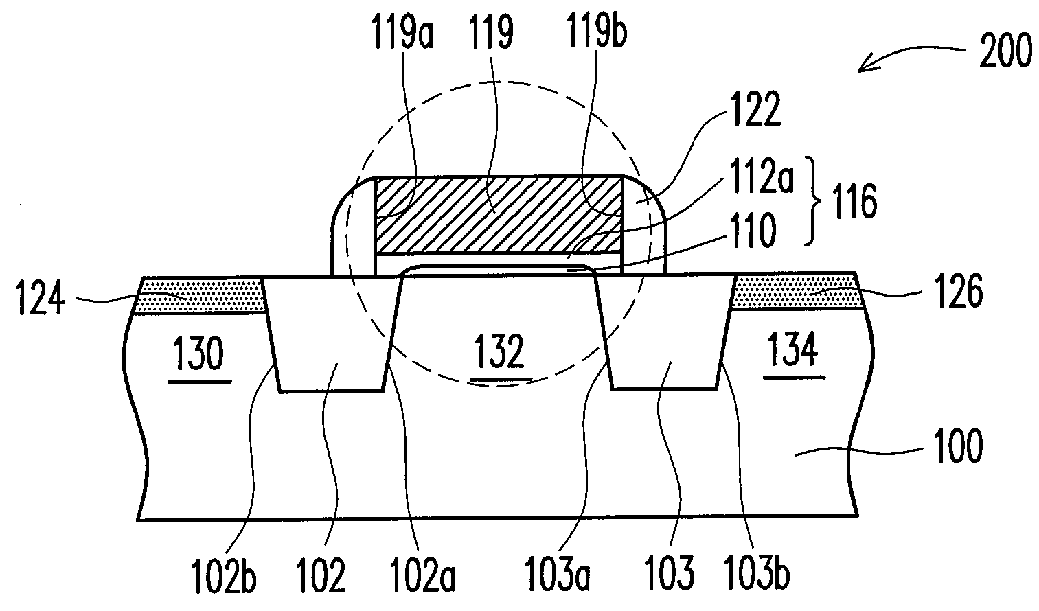
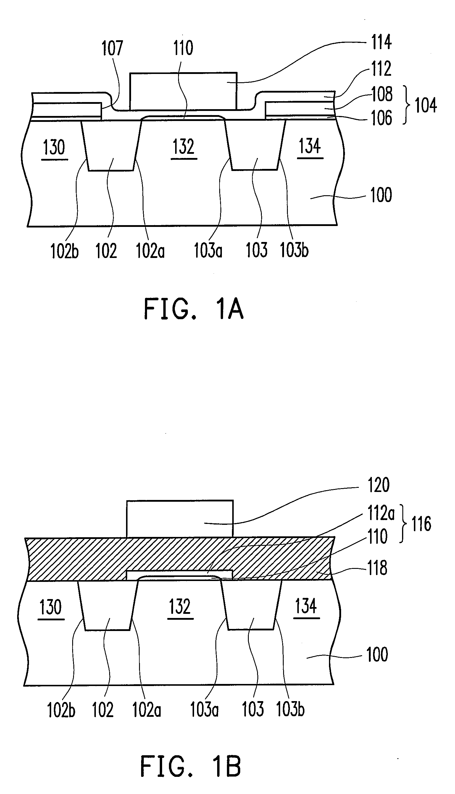
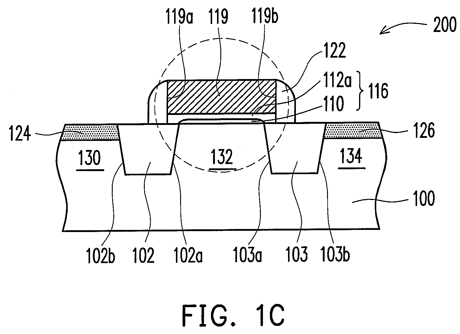
[0038]FIGS. 1A to 1C are schematic, cross-sectional views showing selected steps for the fabrication of a high voltage semiconductor transistor according to an embodiment of the present invention.

[0039]Referring to FIG. 1A, a substrate 100 is provided, wherein a material constituting the substrate 100 includes semiconductor such as silicon or silicon-on-insulator (SOI). In one embodiment, the substrate 100 includes silicon with P type dopants. In one embodiment, a well region (not shown), such as N-type well and / or P-type well, is further formed in the substrate 100. Isolation structures 102, 103 are formed in the substrate 100 to define the active regions 130, 132, 134. Isolation structures 102, 103 are formed by, for example, shallow trench isolation (STI) method.

[0040]A patterned mask layer 104 is then formed on the substrate 100, wherein the patterned mask layer 104 has an opening 107 that exposes the surface of the active region between interior sides 102a, 103a of the isolatio...


PUM


Abstract

A high voltage device is provided. The high voltage device includes a gate on a substrate, two source / drain regions in the substrate beside the gate, and a composite gate dielectric layer that includes at least two stacked continuous layers, extending from one side to another side of the gate. Wherein, the at least two stacked continuous layers is a combination of at least one thermal oxide layer and at least one chemical vapor deposited layer.

Description

BACKGROUND OF THE INVENTION[0001]1. Field of Invention[0002]The present invention relates to an integrated circuit and a method of fabricating the same; more particularly, the present invention relates to a high voltage device that has a pad oxide with a uniform thickness and a method of fabricating the same.[0003]2. Description of Related Art[0004]Metal oxide semiconductor transistor device is the most fundamental unit in a semiconductor device. A typical metal oxide semiconductor transistor includes a gate, a gate oxide layer and source / drain regions. The gate is configured on a substrate, using a gate oxide layer for insulating from the substrate. The source / drain regions are doped regions having the same types of dopants and are configured in the substrate beside two sides of the gate.[0005]A typical method in forming the gate oxide layer is via performing a thermal oxidation process, in which the substrate surface is exposed to oxygen ambient and a silicon oxide layer is formed...

Claims


Application Information

Patent Timeline
Patent Type & Authority Applications(United States)
IPC IPC(8): H01L29/94H01L21/336
CPCH01L21/28167H01L29/513H01L29/4908H01L29/0653
Inventor MA, YUN-HANLEE, MING-TSUNGLIANG, SHIH-MINGCHEN, HWI-HUANG
Owner UNITED MICROELECTRONICS CORP
Features
  • Generate Ideas
  • Intellectual Property
  • Life Sciences
  • Materials
  • Tech Scout
  • Unparalleled Data Quality
  • Higher Quality Content
  • 60% Fewer Hallucinations
Learn More