Multiple cavity etched-facet dfb lasers

a laser device and multi-cavity technology, applied in semiconductor lasers, laser details, laser optical resonator construction, etc., can solve the problems of laser performance and characteristics, lasers have limited design yield, and conventional lithographical techniques cannot be readily used to further process lasers, etc., to achieve accurate determination and increase chip yield

Active Publication Date: 2009-03-12
MACOM TECH SOLUTIONS HLDG INC
View PDF14 Cites 8 Cited by
  • Summary
  • Abstract
  • Description
  • Claims
  • Application Information

AI Technical Summary

Benefits of technology

[0008]The present invention addresses the foregoing issues through provision of an improved structure and method for making etched-facet semiconductor DFB lasers in which at least two DFB laser cavities per chip are formed at close proximity to each other. The cavities are configured such that the first cavity forms a first phase with a diffraction grating and the second cavity forms a second different phase with the diffraction grating. In the preferred embodiment, this phase difference is achieved by making the length of one of the laser cavities slightly longer than the length of the other cavity. Since the relative position of the facets between two closely positioned cavities can be accurately determined in etched facet lasers, by changing the cavity length by a small amount in one of the two laser cavities, the phase between the facet and the diffraction gratings of the DFB lasers will be at or closer to the desired range for one of the at least two lasers. In actual practice of the invention, this arrangement has resulted in a significant increase in chip yield.

Problems solved by technology

Since the semiconductor material is cleaved to form the laser facets, the locations and orientations of the facets are limited; furthermore, once the wafer has been cleaved, it typically is in small pieces so that conventional lithographical techniques cannot readily be used to further process the lasers.
Unfortunately, cleaved facets can only be placed within a desired position only to a few microns causing random phase variation between the facets and the grating, and are therefore unpredictable in laser performance and characteristics.
As such, these lasers have a limited yield by design.
DFB lasers can be processed with photolithographically defined etched facets, but the alignment accuracy of the photolithographic system together with the angular misalignment between the placement of the grating and the etched facet is insufficient to deterministically specify the phase between the facet and the grating across a wafer.

Method used


Image

  • Multiple cavity etched-facet dfb lasers
  • Multiple cavity etched-facet dfb lasers
  • Multiple cavity etched-facet dfb lasers

Examples


Embodiment Construction

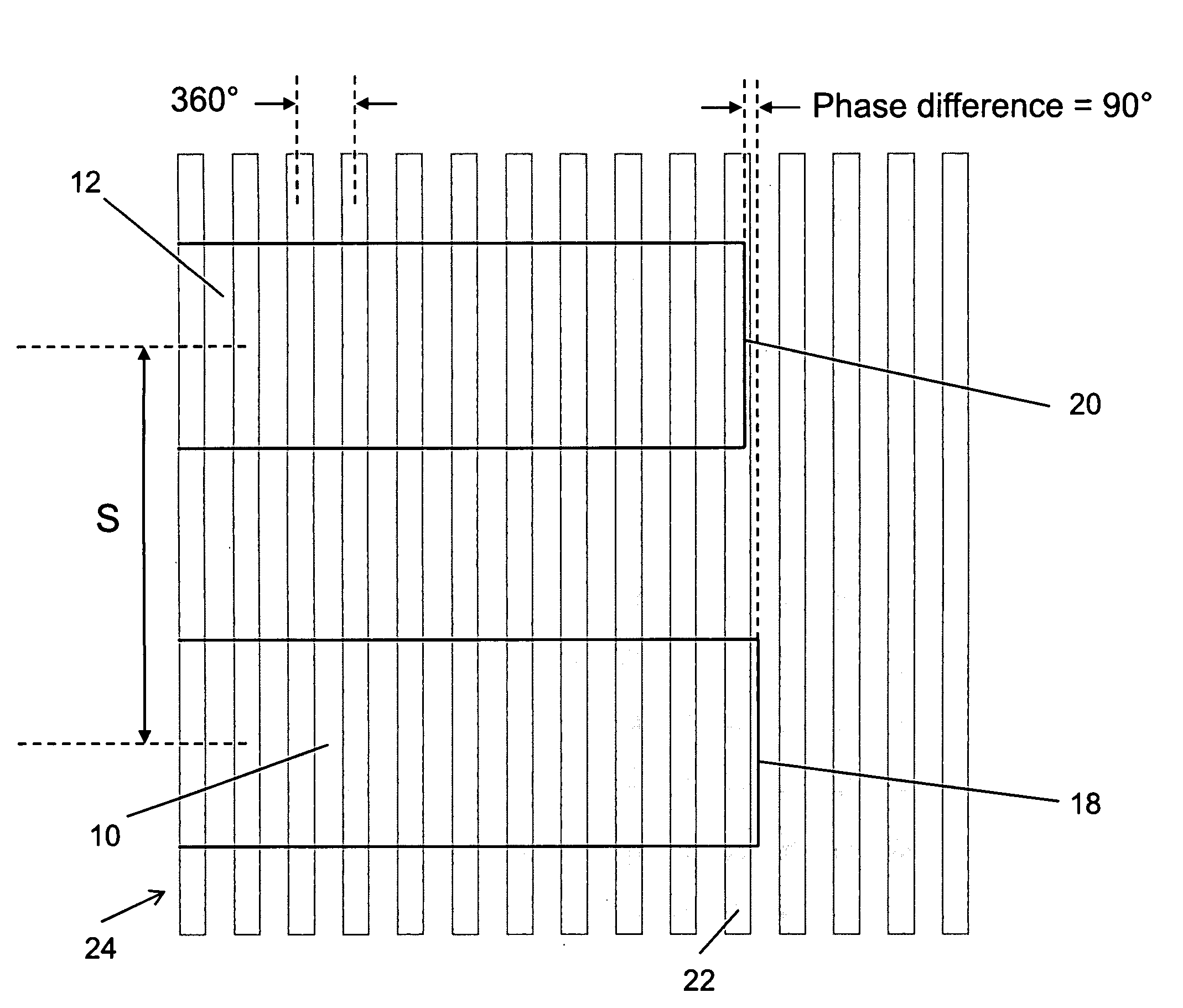
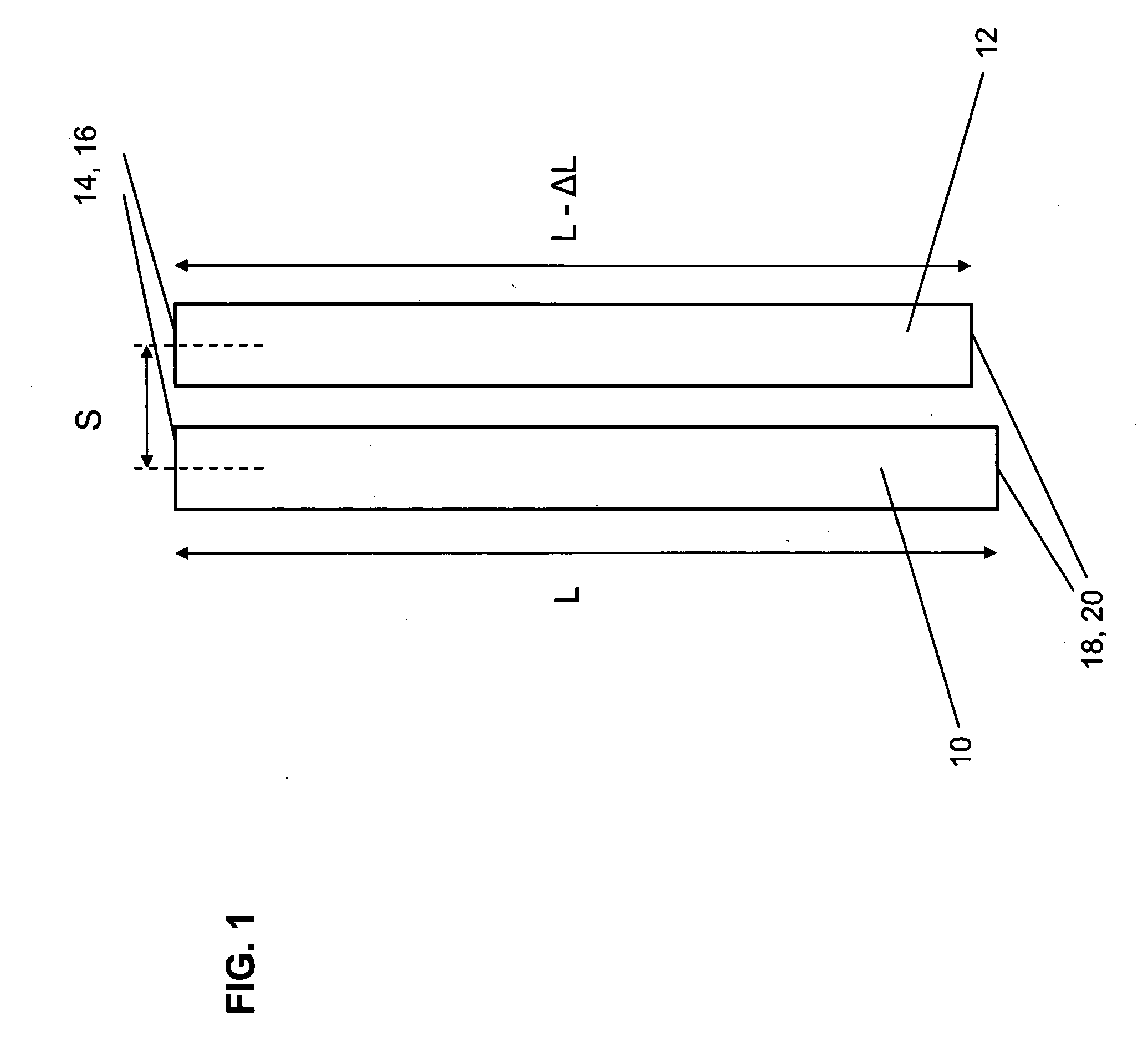
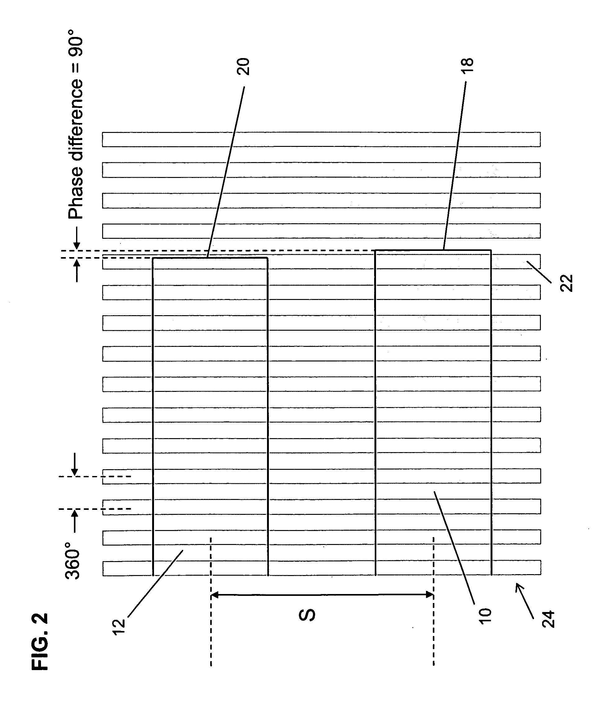
[0016]The present invention can be applied to a DFB semiconductor laser structure to improve the yield during manufacture thereof. The details of the inventive concept are provided herein following a discussion of the known laser structures and fabrication techniques which are preferably employed in the invention. As is conventional, in the fabrication of solid state ridge lasers, the substrate may be formed, for example, of a type III-V compound or an alloy thereof, which may be suitably doped. The substrate includes a top surface on which is deposited, as by an epitaxial deposition such as Metalorganic Chemical Vapor Deposition (MOCVD), a succession of layers which form an optical cavity that includes an active region. Typically, the grating layer will be near the active region (above or below) and will be patterned with a periodic structure through e-beam lithography, holographic lithography, or nano-imprint technology followed by etching to form the gratings in the grating layer...


PUM


Abstract

A semiconductor chip has at least two DFB etched facet laser cavities with one set of facets with AR coatings and a second set of etched facets with HR coatings that have a different relative position with respect to the gratings. This creates a difference in the phase between each of the etched facets and the gratings which changes the operational characteristics of the two laser cavities such that at least one of the lasers provides acceptable performance. As a result, the two cavity arrangement greatly improves the yield of the fabricated chips.

Description

CROSS REFERENCE TO RELATED APPLICATIONS[0001]This application claims the benefit of U.S. Provisional Application No. 60 / 960,014, which was filed on Sep. 11, 2007 and is hereby incorporated by reference in its entirety.FIELD OF THE INVENTION[0002]The present invention relates, in general, to etched-facet photonic devices, and more particularly to multiple cavity etched-facet DFB laser devices.BACKGROUND OF THE INVENTION[0003]Semiconductor lasers typically are fabricated on a wafer by growing an appropriate layered semiconductor material on a substrate through Metalorganic Chemical Vapor Deposition (MOCVD) or Molecular Beam Epitaxy (MBE) to form an epitaxy structure having an active layer parallel to the substrate surface. The wafer is then processed with a variety of semiconductor processing tools to produce a laser optical cavity incorporating the active layer and incorporating metallic contacts attached to the semiconductor material. Laser facets typically are formed at the ends of...

Claims


Application Information

Patent Timeline
Patent Type & Authority Applications(United States)
IPC IPC(8): H01S5/00H01S5/12
CPCH01S5/028H01S5/1021H01S5/18H01S5/12H01S5/4025H01S5/1039
Inventor BEHFAR, ALEX A.GREEN, MALCOLMKWONG, NORMANSTAGARESEN, CRISTIAN
Owner MACOM TECH SOLUTIONS HLDG INC
Why Eureka
Try Eureka