Dense array of field emitters using vertical ballasting structures

a field emitter and ballasting technology, applied in the manufacture of electrode systems, electric discharge tubes/lamps, instruments, etc., can solve the problems of difficult to obtain uniform or high currents from field emitter arrays, unattractive ballasting approaches, and large resistors in series with field emitters, etc., to achieve and high dynamic resistance with large saturation current

Active Publication Date: 2009-03-19
MASSACHUSETTS INST OF TECH
View PDF5 Cites 23 Cited by
  • Summary
  • Abstract
  • Description
  • Claims
  • Application Information

AI Technical Summary

Benefits of technology

[0005]According to one aspect of the invention, there is provided a field emitter structure. The field emitter structure includes a vertical un-gated transistor structure formed on a semiconductor substrate. The semiconductor substrate includes a vertical pillar structure to define said un-gated transistor structure. An emitter structure is formed on said vertical un-gated transistor structure. The emitter structure is positioned in a ballasting fashion on the vertical un-gated transistor structure so as to allow said ungated field effect transistor structure to effectively provide high dynamic resistance with large saturation currents.
[0006]According to another aspect of the invention, there is provided a field emitter array structure. The field emitter array structure includes a plurality of vertical un-gated transistor structures formed on a semiconductor substrate. The semiconductor substrate includes a plurality of vertical pillar structures to define said un-gated transistor structures. A plurality of emitter structures are form...

Problems solved by technology

Attempts to increase the emission current by increasing the voltage often result in burnout and shifting of the operating voltage to higher voltages.
Therefore, it is difficult to obtain uniform or high currents f...

Method used


Image

  • Dense array of field emitters using vertical ballasting structures
  • Dense array of field emitters using vertical ballasting structures
  • Dense array of field emitters using vertical ballasting structures

Examples


Embodiment Construction

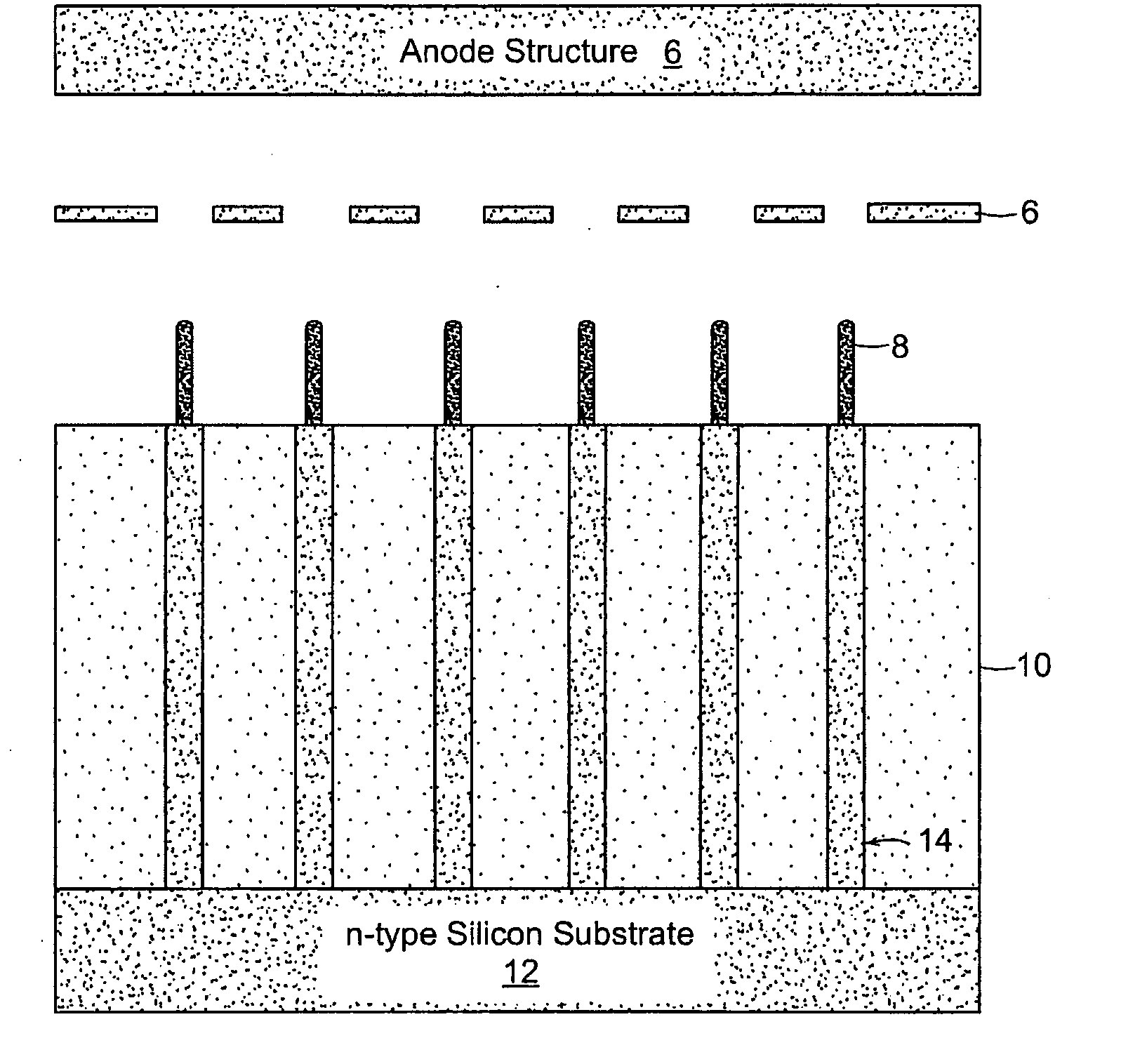
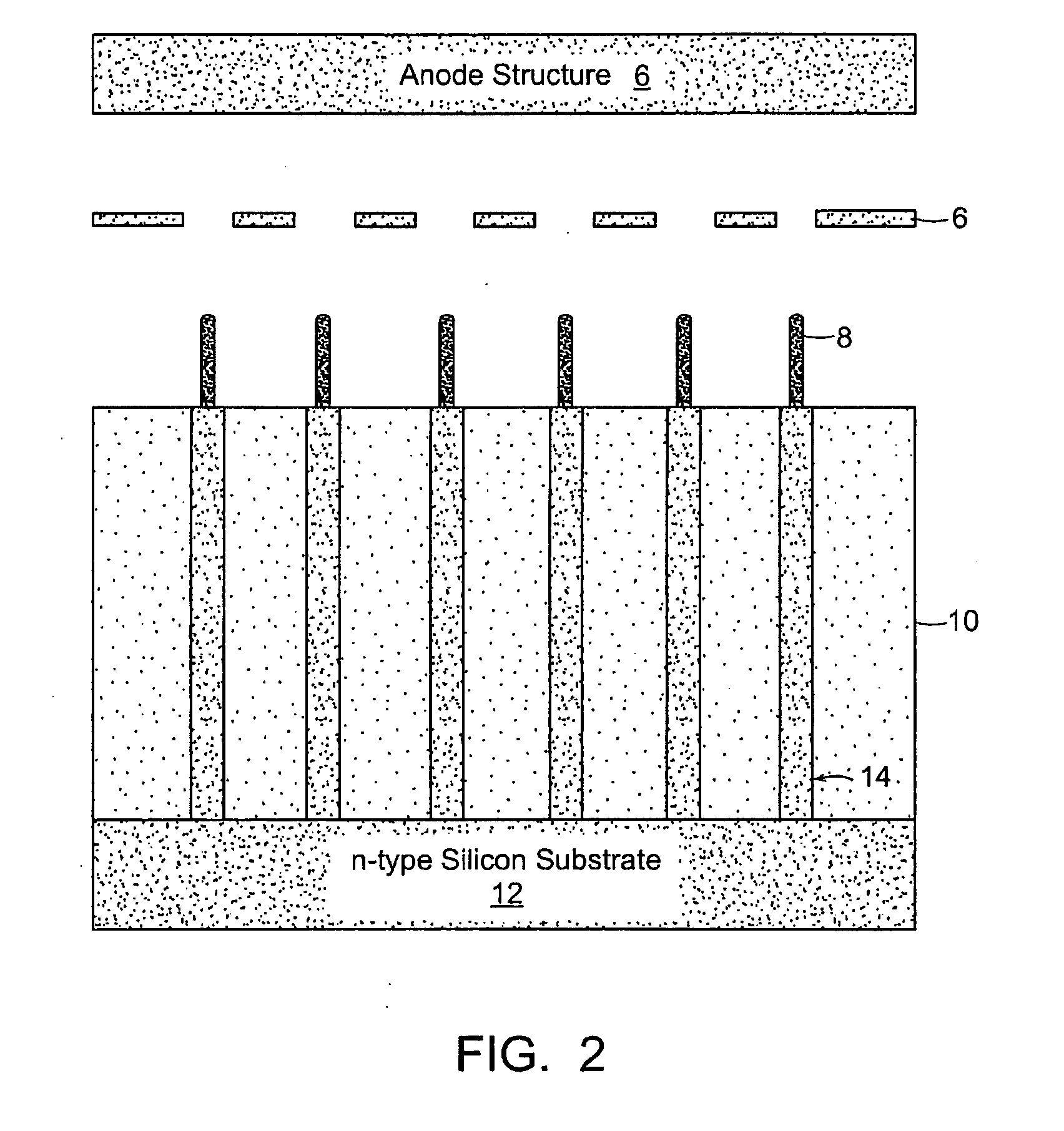
[0026]The invention provides the first dense (106 emitters / cm2) high current (10 mA) array of individually ballasted field emitters that use un-gated field effect transistors (FETs) as current limiters.

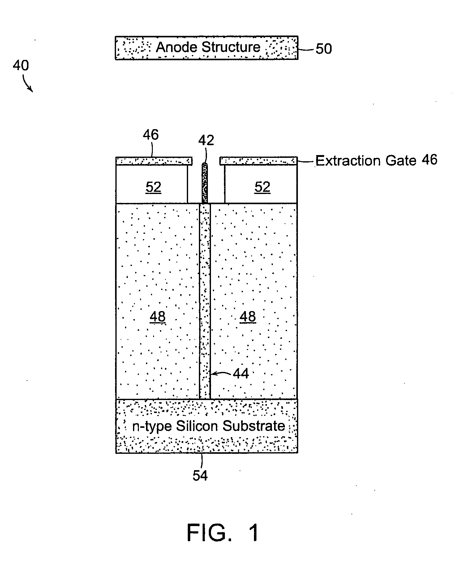
[0027]FIG. 1 show a a field emitter structure individually ballasted with an ungated field effect transistor 40 formed in accordance with the invention. The field emitter structure individually ballasted with an ungated field effect transistor includes an anode 50 and a field emitter 42 being defined by a sharp tip made of metal, semiconductor or any other conducting material individually ballasted by a current source, which in this case is implemented by a semiconductor column / pillar ungated field effect transistor (FET) 44 made on an substrate 54, which is a n-type silicon substrate but other similar materials can be used. The field emitter is preferably self-aligned though not absolutely necessary to annular extraction gates 46 that are close proximity. The ungated FET 44 includes ...


PUM


Abstract

A field emitter array structure is provided. The field emitter array structure includes a plurality of vertical un-gated transistor structures formed on a semiconductor substrate. The semiconductor substrate includes a plurality of vertical pillar structures to define said un-gated transistor structures. A plurality of emitter structures are formed on said vertical un-gated transistor structures. Each of said emitter structures is positioned in a ballasting fashion on one of said vertical un-gated transistor structures so as to allow said vertical ungated transistor structure to effectively provide high dynamic resistance with large saturation currents.

Description

PRIORITY INFORMATION[0001]This application claims priority from provisional application Ser. No. 60 / 973,543 filed Sep. 19, 2007, which is incorporated herein by reference in its entirety.BACKGROUND OF THE INVENTION[0002]The invention is related to the field of field emitter arrays, and in particular to dense arrays of field emitters using vertical ballasting structures. Each field emitter uses a vertical ballasting structure.[0003]Electrons are field emitted from the surface of metals and semiconductors when the potential barrier that holds electrons within the material is deformed by the application of a high electrostatic field. Typically high surface electrostatic fields are obtained by the application of a voltage between a gate structure and a high aspect ratio structure with nano-meter scale tip radius which usually has Gaussian or log-normal distribution. Due to the exponential dependence on tip radius, emission currents are extremely sensitive to tip radii variation. Consequ...

Claims


Application Information

Patent Timeline
IPC IPC(8): H01J1/304H01J9/02
CPCH01J2201/319H01J1/3042
Inventor AKINWANDE, AKINTUNDE I.VELASQUEZ-GARCIA, LUIS FERNANDO
Owner MASSACHUSETTS INST OF TECH
Why Eureka
Try Eureka