Semiconductor storage device including counter noise generator and method of controlling the same

a technology of counter noise generator and storage device, which is applied in the direction of information storage, static storage, digital storage, etc., can solve the problems of reducing the quality of data held, the influence of voltage fluctuation on the noise current generated by the hvdd power source b>930/b>, and the difficulty of dram edram expansion, etc., to reduce the influence of noise current on the reference voltage power source, reduce the noise current generated, and cancel the noise current generated

Inactive Publication Date: 2009-03-19
RENESAS ELECTRONICS CORP
View PDF3 Cites 3 Cited by
  • Summary
  • Abstract
  • Description
  • Claims
  • Application Information

AI Technical Summary

Benefits of technology

[0019]According to the semiconductor storage device of the present invention, it is possible to cancel the noise current generated due to the voltage fluctuation of a counter plate of a capacitor when the data is written in the memory cell by the counter noise current from the counter noise generator, whereby the influence of the noise current on the reference voltage power source can be reduced.
[0020]According to the semiconductor storage device of the present invention, it is possible to reduce the noise current generated due to the voltage fluctuation of the cell node with respect to the reference voltage power source when the data held in the memory cell is rewritten, whereby an output voltage of the reference voltage power source can be made stable.

Problems solved by technology

However, it is difficult to make the DRAM part (eDRAM) larger because total chip area of the system LSI is limited.
However, in a case where the voltage fluctuation due to the rewriting of the data from the H level to the L level is caused in the cell node as described above when the ratio of the number of memory cells in which the data is rewritten to the number of memory cells in which the data is not rewritten is large, as an example, the influence of the noise current generated by the voltage fluctuation on the HVDD power source 930 cannot be ignored.
This may cause degradation of quality of the data held in the capacitor of the memory cell.
Furthermore, the response of the voltage determination circuit in the HVDD power source needs to be enhanced in order to increase the response speed, which increases the power consumption of the amplifier of the voltage determination circuit.
Accordingly, the power consumption of the semiconductor storage device or the area required in the semiconductor storage device increases, which causes an adverse effect.
However, according to this technique, the noise can further be produced before writing depending on the data.
As stated above, according to the semiconductor storage device in the related art, the noise current is generated in the reference voltage power source which is capacity-coupled to the counter plate of the capacitor of the cell node due to the voltage fluctuation of the cell node generated when the data held in the memory cell is rewritten, which makes the output voltage of the reference voltage power source unstable.

Method used


Image

  • Semiconductor storage device including counter noise generator and method of controlling the same
  • Semiconductor storage device including counter noise generator and method of controlling the same
  • Semiconductor storage device including counter noise generator and method of controlling the same

Examples


first embodiment

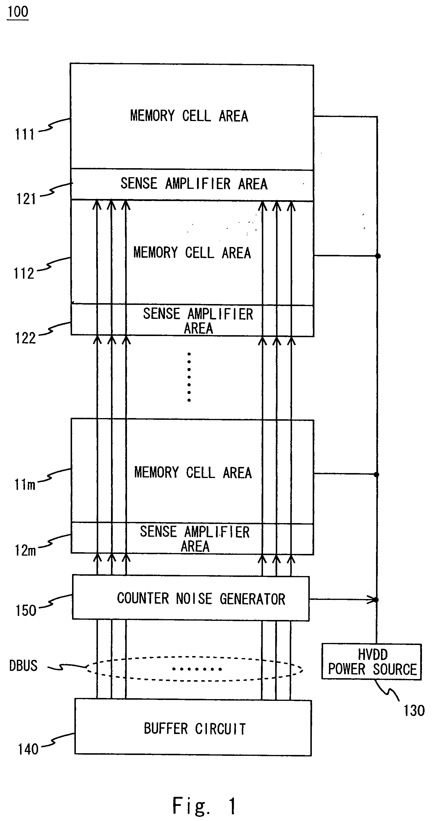
[0033]The first embodiment to which the present invention is applied will now be described in detail with reference to the drawings. The first embodiment is the one in which the present invention is applied to the DRAM.

[0034]FIG. 1 shows one example of a schematic configuration diagram of a DRAM 100. The DRAM 100 includes memory cell areas 111, 112, . . . , 11m where a plurality of memory cells are arranged, sense amplifier areas 121, 122, . . . , 12m, an HVDD power source 130 having an output voltage of VDD / 2, a buffer circuit 140 (buffer circuit in a broad sense) , and a counter noise generator 150. Data written into the memory cell is transferred to the memory areas (111, 112, . . . , 11m) from the buffer circuit 140 through each of the sense amplifier areas (121, 122, . . . , 12m) by common data lines DBus (True / Bar). When the number of I / Os is “×256 bits”, for example, it means that there are 256 common data lines DBus (True / Bar) or 512 lines with both of the True and Bar.

[0035...

second embodiment

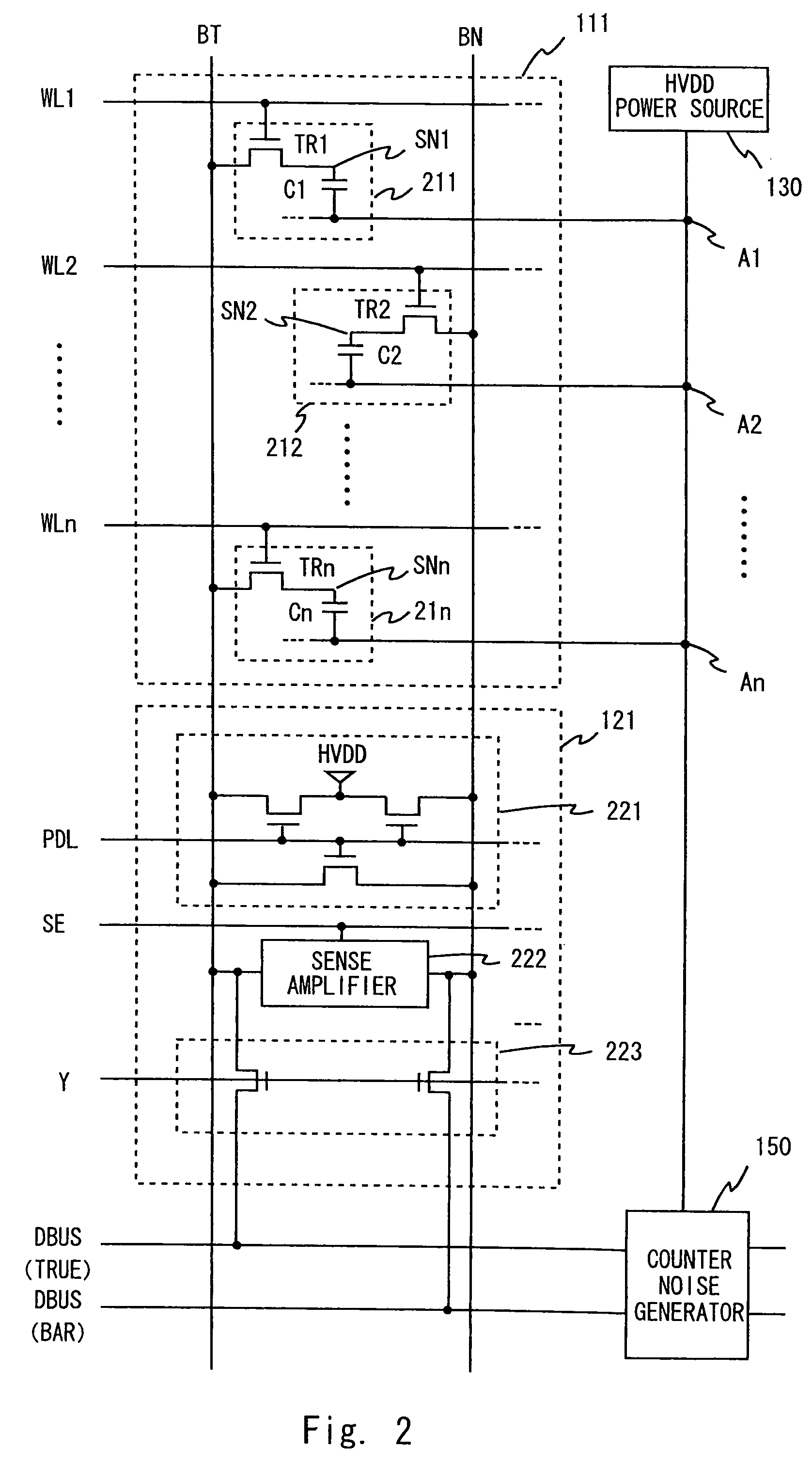
[0065]The second embodiment to which the present invention is applied will be described in detail with reference to the drawings. The second embodiment is the one in which the present invention is applied to the DRAM as the same as in the first embodiment. The configuration in the second embodiment is substantially the same as that in the first embodiment except that the current amount of the counter noise current output from the counter noise generator 150 is calculated only from the written data held in the buffer circuit 140. Therefore, the circuit configuration is the same as in FIGS. 1 and 2 described in the first embodiment. In the second embodiment, only a part which is different from the first embodiment will be described, and the description of the circuit configuration or the like will be omitted.

[0066]FIG. 6 shows a timing chart showing a circuit operation of FIG. 2 in the second embodiment. Now, a case will be described in which the “L” data is held in the memory cell 21...


PUM


Abstract

A semiconductor storage device according to one aspect of the present invention includes a reference voltage source connected to a capacitor of a cell included in a memory, a buffer circuit holding data to be written in the cell, and a counter noise generator outputting a counter noise current canceling a noise current generated by rewriting the data in the cell to the reference voltage source according to the data held in the buffer circuit.

Description

BACKGROUND OF THE INVENTION[0001]1. Field of the Invention[0002]The present invention relates to a semiconductor storage device including a counter noise generator and a method of controlling the same.[0003]2. Description of Related Art[0004]A DRAM (Dynamic Random Access Memory) includes complementary bit lines arranged in perpendicular to word lines, and memory cells arranged in intersections of the word lines and the complementary bit lines in matrix form.[0005]FIG. 9 shows one example of a schematic configuration diagram of a related DRAM 900. The DRAM 900 includes memory cell areas (911, 912, . . . , 91m) where a plurality of memory cells are arranged, sense amplifier areas (921, 922, . . . , 92m) , an HVDD power source 930 (output voltage VDD / 2) , and a buffer circuit 940. Data written into the memory cells are transferred to the memory areas (911, 912, . . . , 91m) from the buffer circuit 940 through each of the sense amplifier areas (921, 922, . . . , 92m) by common data line...

Claims


Application Information

Patent Timeline
Patent Type & Authority Applications(United States)
IPC IPC(8): G11C7/00
CPCG11C11/4074G11C7/02
Inventor TAKAHASHI, HIROYUKI
Owner RENESAS ELECTRONICS CORP
Why Eureka
Try Eureka