Electromagnetic wave absorbing and shielding film, method of manufacturing the same, and cable including the same

Inactive Publication Date: 2009-03-19
EMPKO CO LTD
View PDF0 Cites 29 Cited by
  • Summary
  • Abstract
  • Description
  • Claims
  • Application Information

AI Technical Summary

Benefits of technology

[0022]The present invention provides an electromagnetic wave absorbing and shielding film and a method of manufacturing the same comprising forming a plate-like metal flake using a metal powder or ferrite powder, dispersing the metal flake into a binder solution, coating the resulting solution in which the metal flake is dispersed on a

Problems solved by technology

Recently, with the rapid increase the use of various electrical and electronic devices, there arises a problem of electronic noise or electromagnetic interference (EMI).
Such electromagnetic wave absorbers include a rubber sheet using a metal compound; however, since the rubber sheet comprises inorganic materials and polymers mechanically mixed, it has some problems in that its properties are sensitive, heat resistance is decreased, and thus the efficiency of absorbing electromagnetic wave is reduced.
Especially, in the case of such a rubber sheet, since a resin containing chlorine-polyethylene (halogens) is employed, it may cause damage to the human bodies and peripheral devices due to toxic gases such as Cl, F, and the like.
Moreover, since most existing electromagnetic wave absorbers are formed of basic materials such as carbon, ferrite, metal, and the like, they have various problems in that the process is difficult, it is hard to adjust the thickness of the absorber, they are not competitive in price due to high manufacturing co

Method used


Image

  • Electromagnetic wave absorbing and shielding film, method of manufacturing the same, and cable including the same
  • Electromagnetic wave absorbing and shielding film, method of manufacturing the same, and cable including the same
  • Electromagnetic wave absorbing and shielding film, method of manufacturing the same, and cable including the same

Examples


experimental example 1

[0071]The communication cables manufactured in accordance with the Examples and the Comparative Examples were tested as follows to evaluate the workability, the transmission state, the electromagnetic compatibility and the appearance state, and the results are shown in Table 2.

[0072]Workability

[0073]The workability was evaluated whether or not the operation was carried out satisfactorily without any problems such as breakage during the manufacturing of the communication cables using the electromagnetic wave absorbing and shielding films in accordance with the Examples and the Comparative Examples, and designated as suitable or unsuitable.

[0074]Burst Test

[0075]The burst test was carried out whether or not the communication data transmission of the cables were satisfactory by transmitting data until the data transmission was completed using Noise Ken FNS-AX2 equipment, and designated as good or bad.

[0076]CS Signal Transmission Test

[0077]The test was carried out whether or not the CS s...

experimental example 2

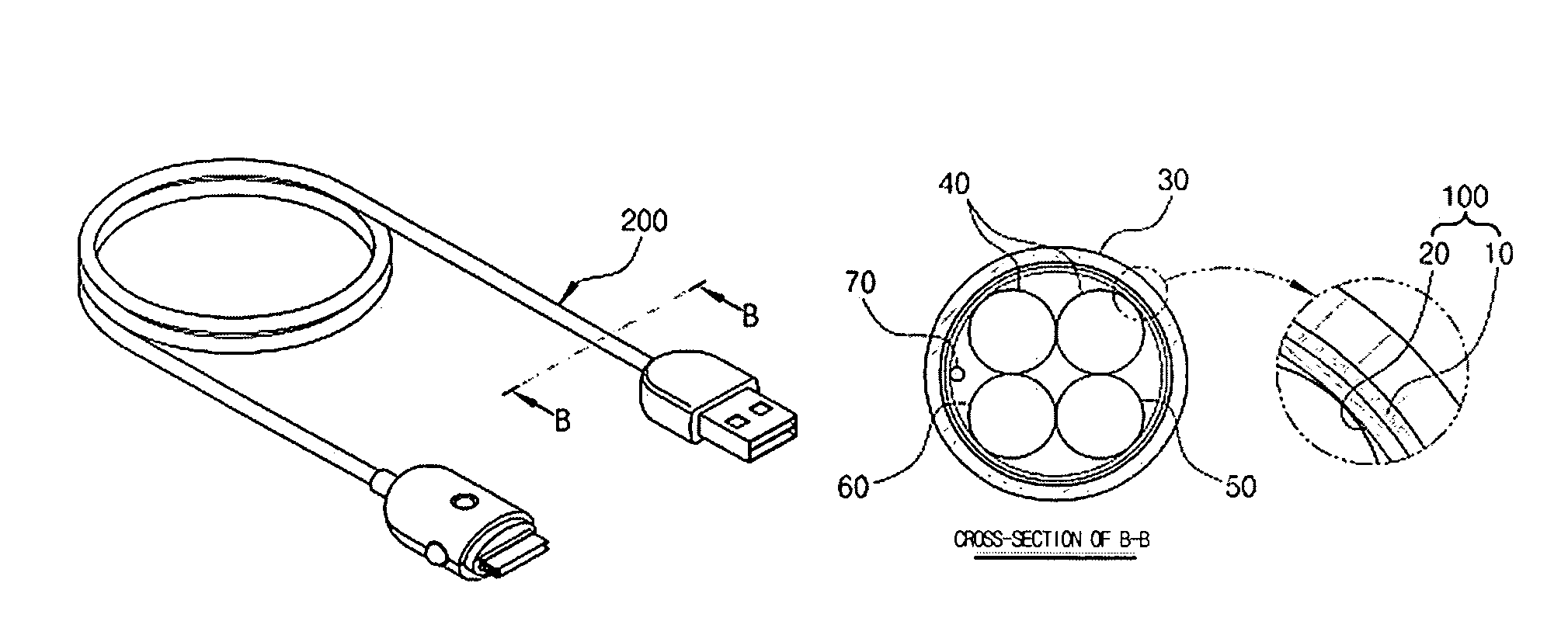
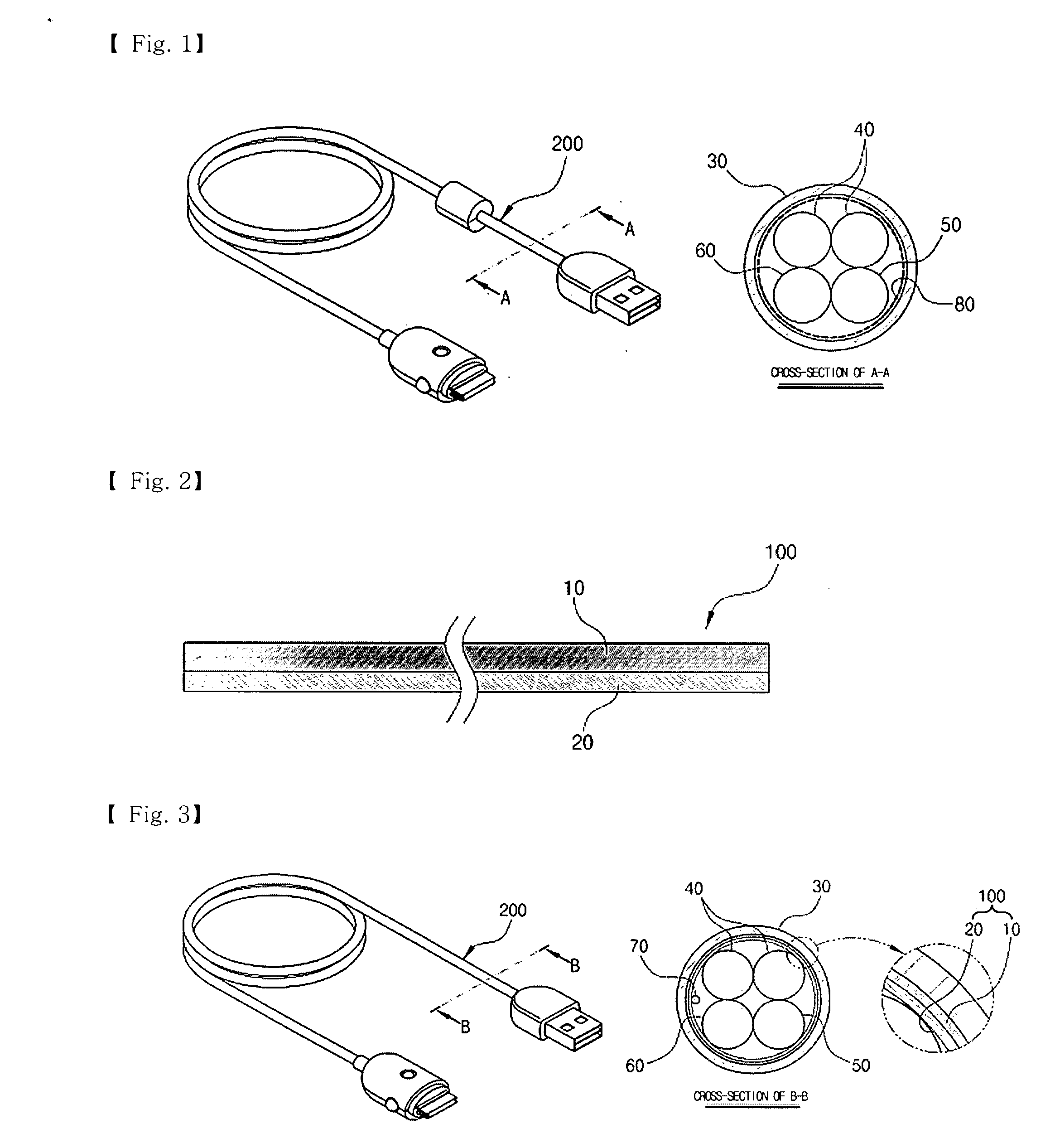
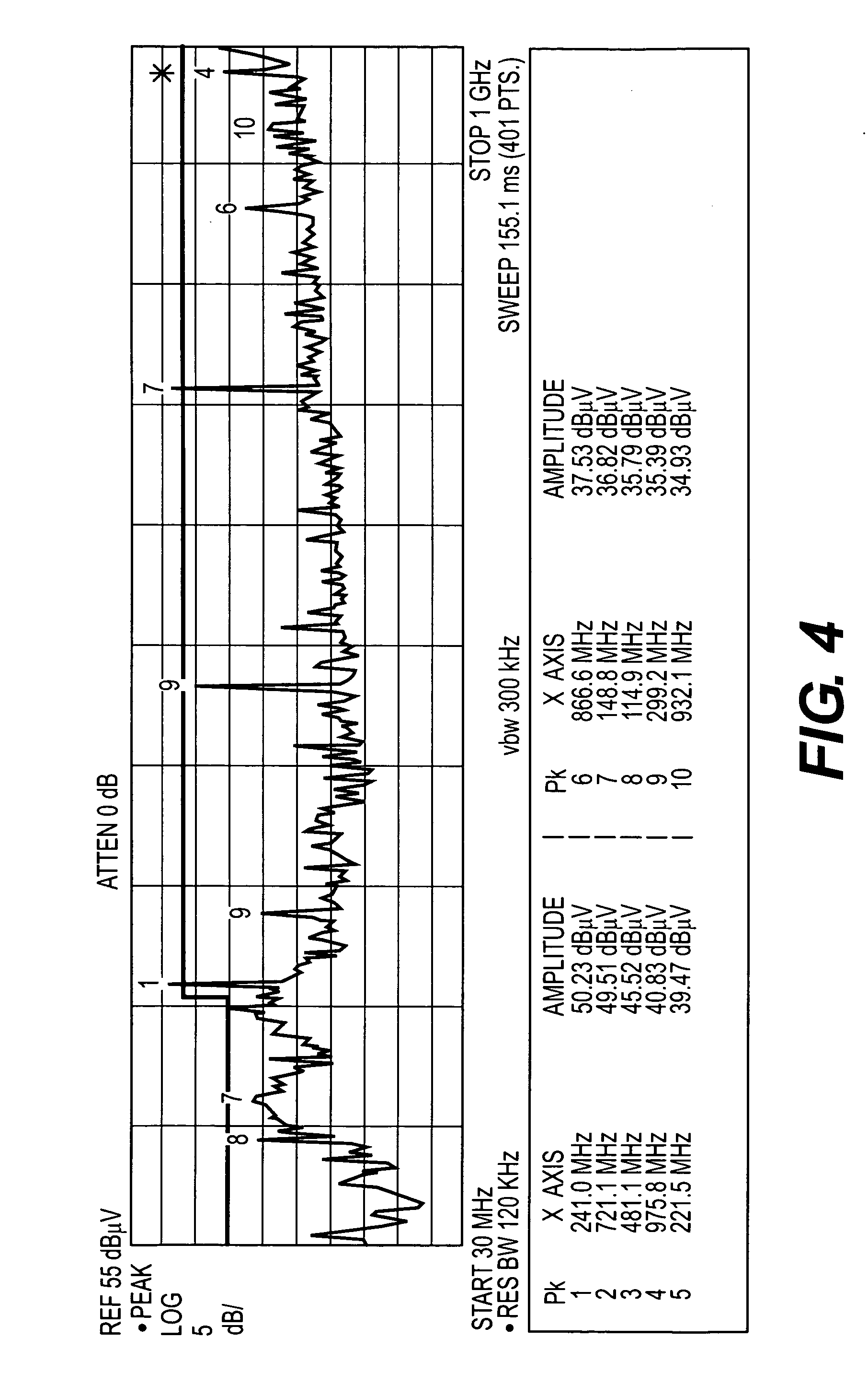
[0083]The electromagnetic wave absorbing and shielding film of the present invention was installed inside an insulating coating of USB cable of Samsung Techwin digital camera NV-1-83. That is, communication lines, a power line and an earth wire provided in the USB cable were wrapped with a strip type electromagnetic wave absorbing and shielding film, in which an electromagnetic wave shielding layer having a thickness of 30 μm and an electromagnetic wave absorbing layer having a thickness of 50 μm were bonded. The electromagnetic wave shielding layer was connected to the earth wire with a silver drain wire, and then the electromagnetic compatibility test was carried out in an EMI chamber (shield performance: MIL-STD-285; conforming to the site attenuation characteristics defined by ANSI C63.4) using EMC analyzer E7403A equipment. As can be seen from the results shown in FIG. 5, the results did not exceed the maximum reference value (red line).

[0084]On the other hand, in the case wher...


PUM

PropertyMeasurementUnit
Lengthaaaaaaaaaa
Lengthaaaaaaaaaa
Lengthaaaaaaaaaa

Abstract

Disclosed herein are an electromagnetic wave absorbing and shielding film, a method of manufacturing the same, and a cable including the electromagnetic wave absorbing and shielding film. The electromagnetic wave absorbing and shielding film includes an electromagnetic wave absorbing layer, in which a plate-like metal flake is formed using a metal powder in the form of a paste or ink, and an electromagnetic wave shielding layer attached to the electromagnetic wave absorbing layer, thus absorbing and shielding electromagnetic wave and reducing noise.
For this, the present invention provides a method of manufacturing an electromagnetic absorbing and shielding film, in which the method includes forming a plate-like metal flake using a spherical metal alloy by an attrition mill, which operates at a predetermined speed for a predetermined time, with the addition of steel use stainless (SUS) balls or ceramic balls and surfactants, and washing the plate-like metal flake with ethyl alcohol, methyl alcohol or water and drying the washed metal flake, the method including: mixing the metal flake powder with resin in a ratio of 30 to 95 wt %:70 to 5 wt % using a mixer and stirring the same to form a metal paste; and coating the metal paste on an electromagnetic wave shielding layer, and a communication cable including the thus formed electromagnetic wave absorbing and shielding film.

Description

CROSS-REFERENCE TO RELATED APPLICATION[0001]This application claims the benefit of Korean Patent Application No. 10-2007-0092899, filed on Sep. 13, 2007, the entire disclosure of which is hereby incorporated by reference.BACKGROUND OF THE INVENTION[0002]1. Field of the Invention[0003]The present invention relates to an electromagnetic wave absorbing and shielding film and, more particularly, to an electromagnetic wave absorbing and shielding film, in which an electromagnetic wave absorbing layer capable of absorbing electromagnetic wave is formed on a support capable of shielding electromagnetic wave, a method of manufacturing the same, and a cable including the electromagnetic wave absorbing and shielding film.[0004]2. Description of Related Art[0005]Recently, with the rapid increase the use of various electrical and electronic devices, there arises a problem of electronic noise or electromagnetic interference (EMI). Such noises may be classified into conduction noise, emission or ...

Claims


Application Information

Patent Timeline
IPC IPC(8): B32B7/00B05D5/12B32B37/00H01B13/00
CPCB32B15/08Y10T428/263B32B2037/243B32B2038/0092B32B2309/105H05K9/0098B32B15/20B32B27/281B32B27/34B32B27/36B32B27/365B32B2307/202B32B2457/00Y10T428/265Y10T428/264B32B37/203H01B11/06
Inventor PYO, JUNG SEOKLEE, JONG YOUNG
Owner EMPKO CO LTD
Why Eureka
Try Eureka