

Magnetoresistive element and magnetic memory
a magnetic memory and element technology, applied in the field of magnetoresistive element and magnetic memory, can solve the problems of increasing the magnetic field required, limited current that can be supplied to the interconnection, and difficult to reduce the current and advance the micropatterning at the same tim
- Summary
- Abstract
- Description
- Claims
- Application Information
AI Technical Summary
Problems solved by technology
Method used
Image

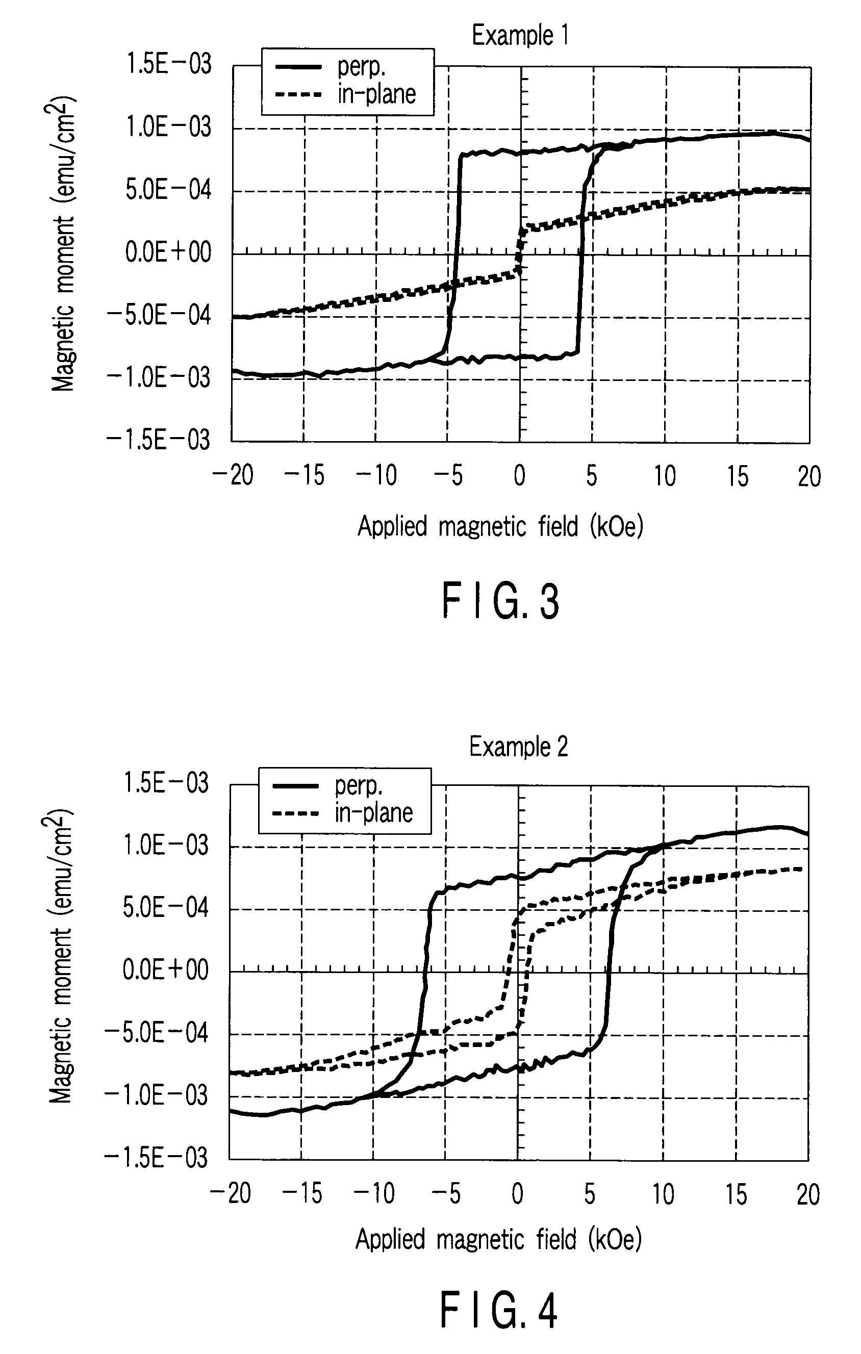
Examples
first embodiment
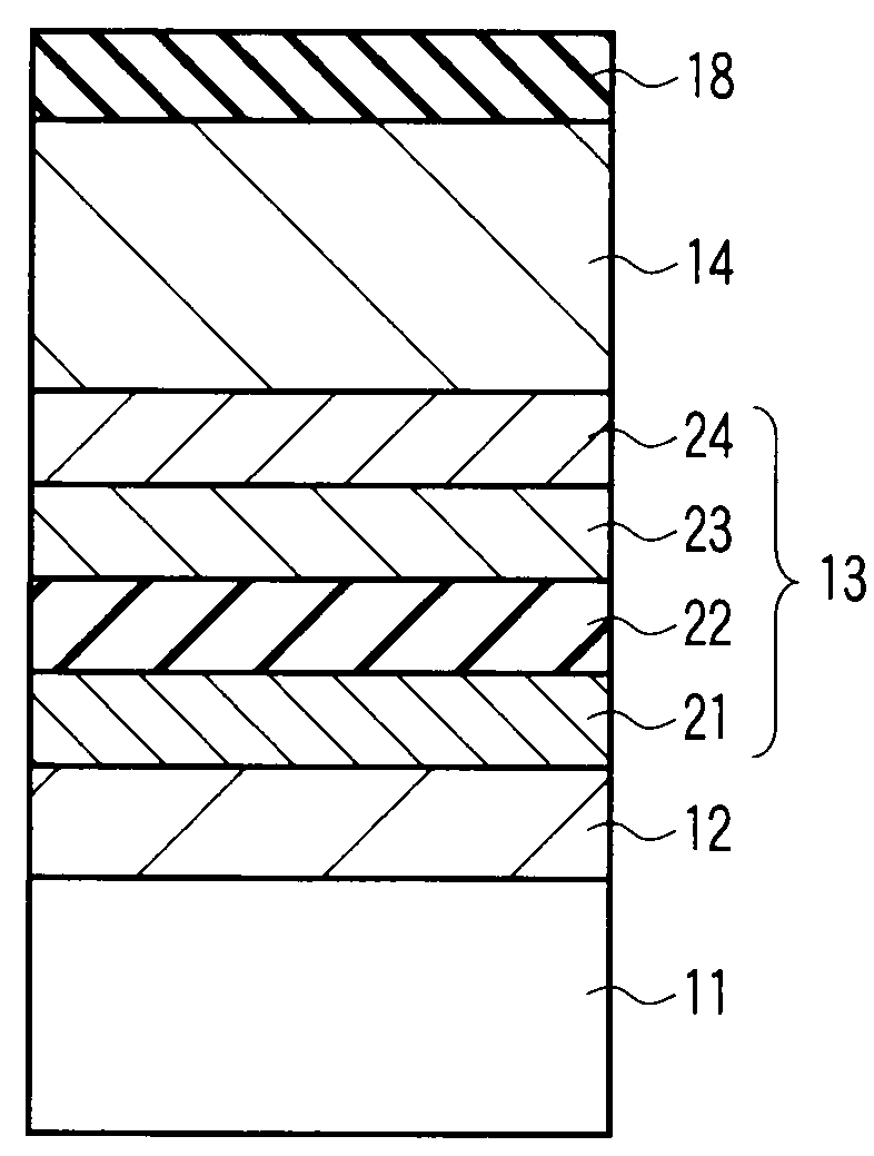
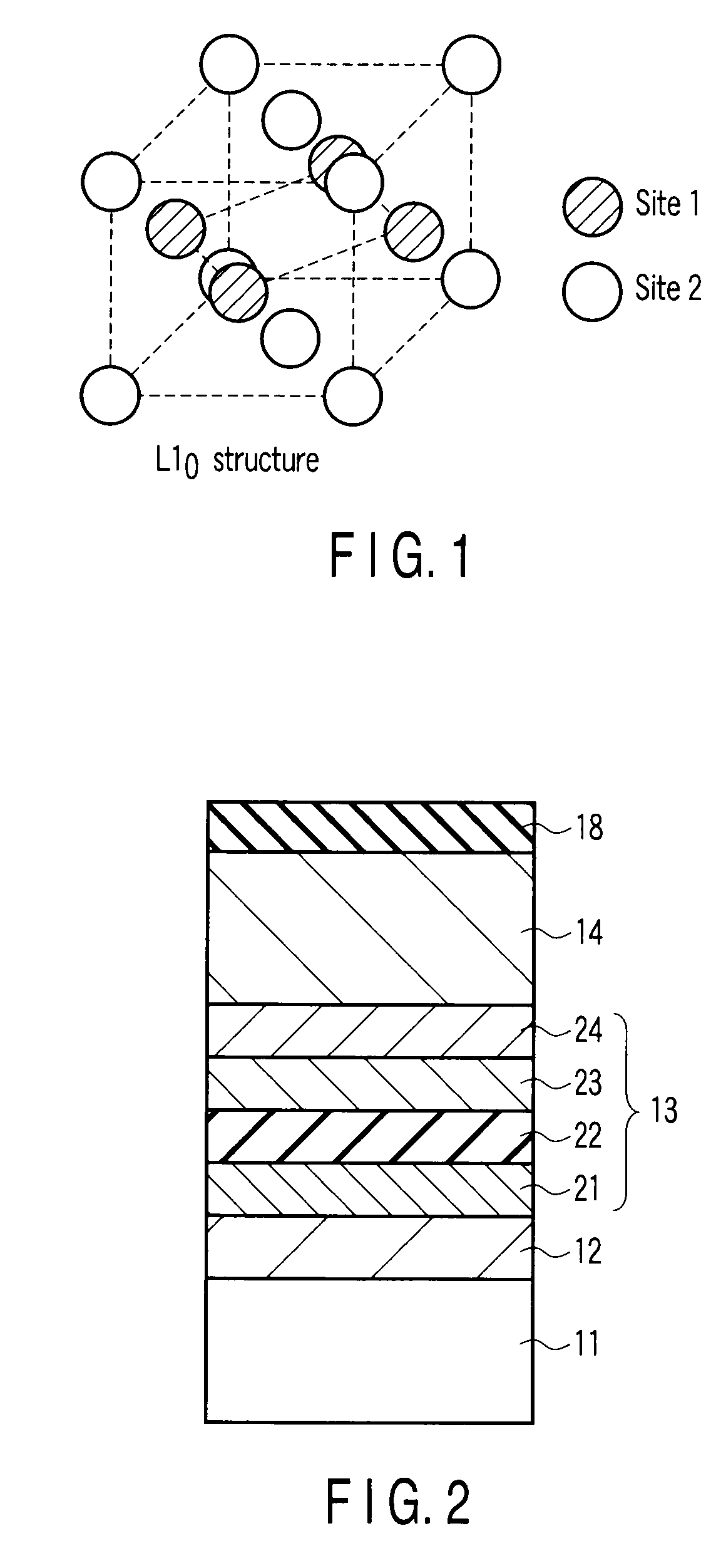
[1] Arrangement of Underlying Layer Made of Ferromagnetic Alloy Having L10 Structure
[0049]L10 is an expression by “Strukturebereichi”, and is also called a CuAu I type in accordance with a representative system of this structure. As shown in FIG. 1, the L10 structure is formed in an alloy containing two or more components when these component elements occupy two face-centered points (sites 1) and remaining face-centered points and corner points (sites 2) of a face-centered cubic lattice at different probabilities. Sites 1 and sites 2 are equal in number, and the stoichiometric composition of the structure is 50 at %. In various alloys that form face-centered cubic solid solutions, the L10 structure appears near the symmetric composition.
[0050]When the constituent elements take this ordered arrangement on the lattice points, (002) or (110) planes equivalent in the face-centered cubic lattice are classified into (001) or (110) planes occupying only sites 1 or 2, and the symmetry of th...
second embodiment
[0172]The second embodiment is an example in which an MRAM is formed by using the MTJ element 10 according to the first embodiment.
[0173]FIG. 23 is a circuit diagram illustrating the arrangement of the MRAM according to the second embodiment of the present invention. This MRAM has a memory cell array 50 including memory cells MC arranged in a matrix. In the memory cell array 50, bit line pairs BL and / BL are formed such that each bit line runs in the column direction. Also, word lines WL are formed in the memory cell array 50 such that each word line runs in the row direction.
[0174]The memory cells MC are arranged at the intersections of the bit lines BL and word lines WL. Each memory cell MC comprises the MTJ element 10, and a selection transistor 51 that is an N-channel MOS transistor. One terminal of the MTJ element 10 is connected to the bit line BL. The other terminal of the MTJ element 10 is connected to the drain terminal of the selection transistor 51. The gate terminal of t...
application example 1
[0186]FIG. 25 specifically shows a digital subscriber line (DSL) data path portion of a DSL modem. This modem comprises a programmable digital signal processor (DSP) 100, analog-to-digital (A / D) converter 110, digital-to-analog (D / A) converter 120, transmission driver 130, reception amplifier 140, and the like.
[0187]No bandpass filter is shown in FIG. 25. Instead, FIG. 25 shows an MRAM 170 of this embodiment and an EEPROM 180 as various types of optional memories for storing a line code program (a program to be executed by the DSP to select and operate a modem in accordance with, e.g., coded subscriber line information and transmission conditions (line codes: QAM, CAP, RSK, FM, AM, PAM, DWMT, and the like)).
[0188]Note that this application example uses two types of memories, i.e., the MRAM 170 and EEPROM 180 as memories for storing the line code program. However, the EEPROM 180 may also be replaced with an MRAM. That is, it is also possible to use only MRAMs instead of using two typ...
PUM
| Property | Measurement | Unit |
|---|---|---|
| thick | aaaaa | aaaaa |
| thick | aaaaa | aaaaa |
| thick | aaaaa | aaaaa |
Abstract
Description
Claims
Application Information