Magnetoresistance effect element and magnetic random access memory

a random access memory and magnetoresistance effect technology, applied in the field of magnetoresistance effect elements and magnetic random access memory, can solve the problems of increasing the chip area, increasing the power consumption of writing, and inferiority of mram to other random access memory in competitiveness, so as to achieve sufficient reduction of write current, the effect of reducing the current density and sufficiently reducing the write curren

Active Publication Date: 2010-07-29
NEC CORP
View PDF6 Cites 42 Cited by
  • Summary
  • Abstract
  • Description
  • Claims
  • Application Information

AI Technical Summary

Benefits of technology

[0010]Therefore, an object of the present invention is to provide a magnetoresistance effect element achieving magnetization reversal based on the current-driven domain wall phenomenon, in which the write current is sufficiently reduced and the current density itself is also reduced, and to provide an MRAM using such a magnetoresistance effect element as a memory cell.

Problems solved by technology

In this case, the chip area is inevitably increased, and power consumption necessary for writing is also increased; this results in that the MRAM is inferior to the other random access memories in competitiveness.
In general, however, an insulating layer is provided between the first and second magnetic layers, and a relatively large current should be flowed through the insulating layer in writing; this causes a problem in rewriting resistance or reliability.
That is, it can be said that the spin injection magnetization reversal is superior in terms of scaling, but has some barriers for practical application.
It is concerned, however, that the absolute value of the write current may be relatively large in the MRAM using the current-driven domain wall motion phenomenon.
Also, to induce the current-driven domain wall motion, a width of the layer in which the domain wall motion occurs should be reduced to a few 10 s nm or less; however, this involves a large difficulty in fabrication technique.
In addition, influences of electron migration and temperature rising may be issues, regarding the use of the current density close to 1×10⁸ [A / cm2] for the domain wall motion.

Method used


Image

  • Magnetoresistance effect element and magnetic random access memory
  • Magnetoresistance effect element and magnetic random access memory
  • Magnetoresistance effect element and magnetic random access memory

Examples


first exemplary embodiment

(Configuration of Magnetoresistance Effect Element)

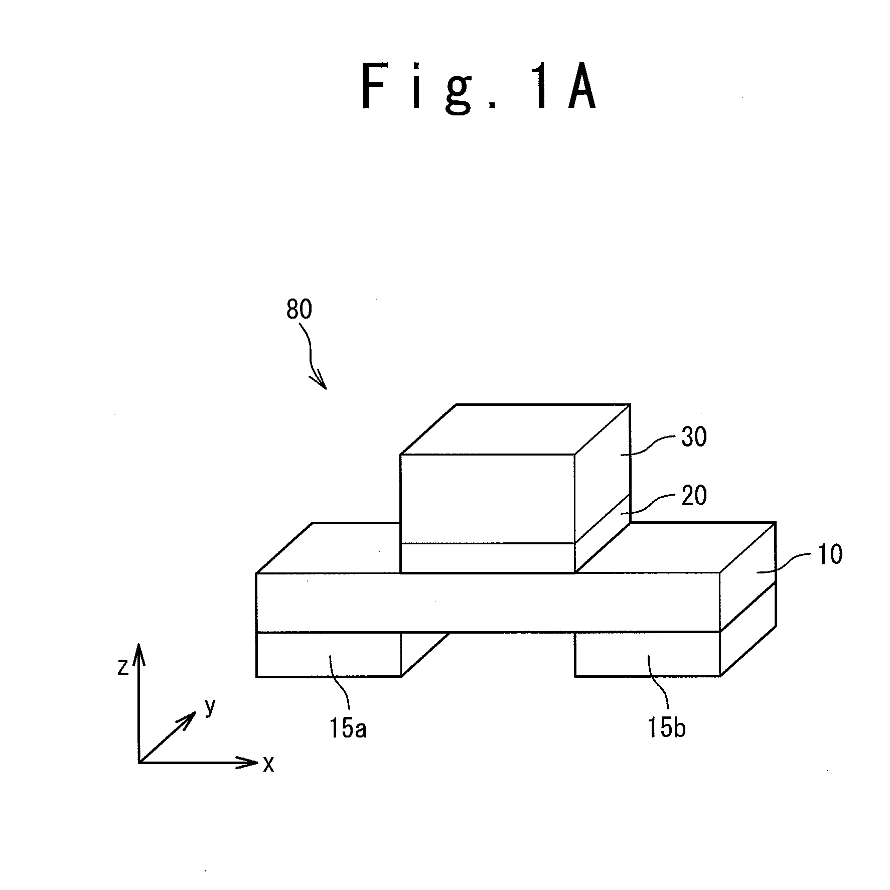
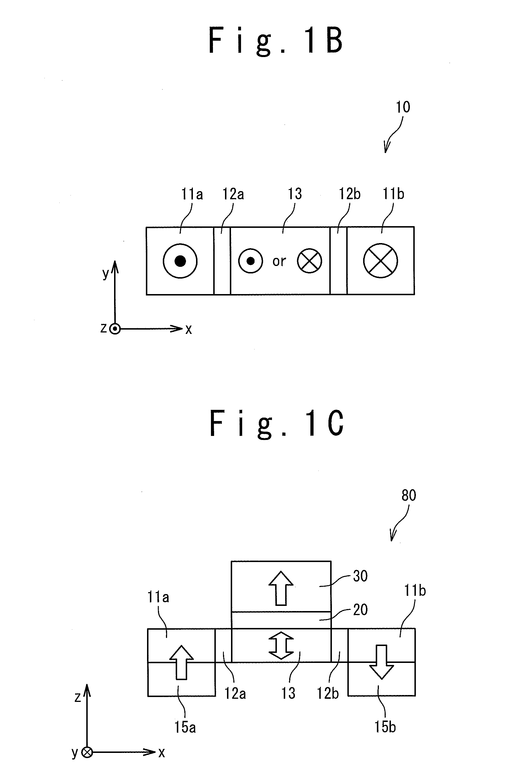
[0054]FIG. 1A is a perspective view illustrating the configuration of a main portion of a magnetoresistance effect element 80 in a first exemplary embodiment of the present invention. In the following, a description is given with an xyz Cartesian coordinate system defined as illustrated in FIG. 1A. FIG. 1B is an x-y plan view illustrating the configuration of the magnetoresistance effect element 80, and FIG. 1C an x-z cross-sectional view illustrating the configuration of the magnetoresistance effect element 80.

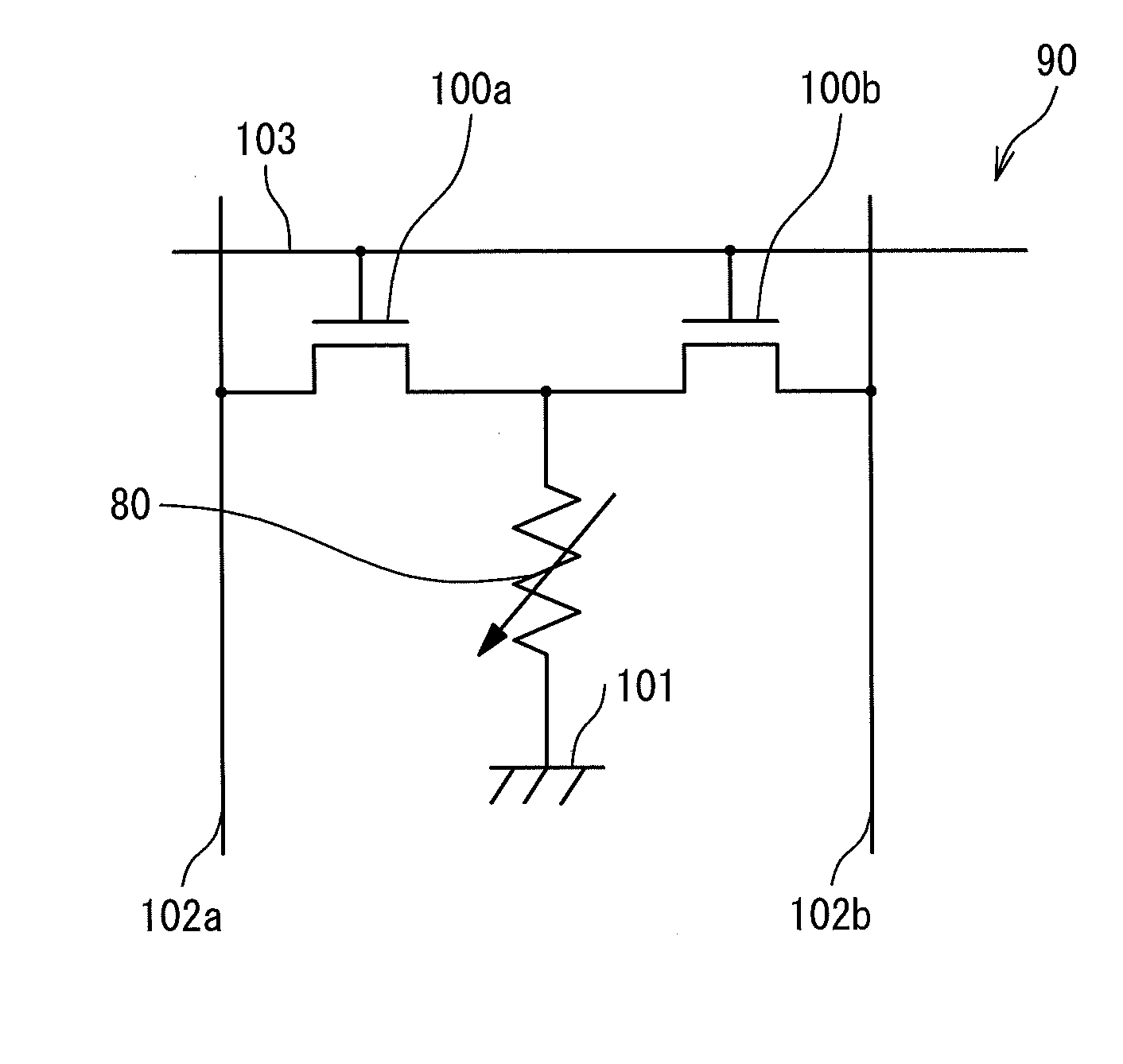
[0055]As illustrated in FIG. 1A, the magnetoresistance effect element 80 includes: a magnetization free layer 10 extending in the x direction; a spacer layer 20 provided adjacent to the magnetization free layer 10; a first magnetization fixed layer 30 provided adjacent to the spacer layer 20 on the opposite side of the magnetization free layer 10; and second magnetization fixed layers 15a and 15b provided adjacent to the both...

second exemplary embodiment

[0103]FIGS. 12A and 12B schematically illustrate structures of the magnetoresistance effect element 80 in a second exemplary embodiment of the present invention, in particular, structures of the magnetization free layer 10. The magnetoresistance effect element 80 of the second exemplary embodiment is related to domain wall pinning sites 12a and 12b in the magnetization free layer 10, and formed such that the domain wall pinning sites 12a and 12b bind the domain wall more strongly.

[0104]As illustrated in FIG. 12A, modulation of the planar shape in the x-y plane provides strong binding of the domain wall. Although FIG. 12A is an exemplary embodiment in which the magnetization free layer 10 is patterned with notches, projections or the like may be provided alternatively. Also, as illustrated in FIGS. 12B and 12C, modulation of the cross-sectional shape in the x-z cross-section provides strong binding of the domain wall at the domain wall pinning site 12a or 12b. As illustrated in FIG. ...

third exemplary embodiment

[0106]FIGS. 13A to 13D schematically illustrate structures of the magnetoresistance effect element 80 in a third exemplary embodiment of the present invention, in particular structures of the magnetization free layer 10. The third exemplary embodiment is related to the shape of the magnetization free layer 10, and achieves notably stable binary states.

[0107]In the case of the perpendicular magnetization film, a state where the domain wall stops in the middle of the domain wall motion portion 13 is not so unstable. Such state, which is an intermediate state between “0” and “1”, should be avoided. Meanwhile, the domain wall tends to move in a direction that decreases the area thereof as much as possible to reduce the energy of the entire system. Accordingly, when a portion at the middle of the domain wall motion portion 13 has a wider width than the other parts, the portion becomes unstable, and therefore the intermediate state described above is eliminated. Schematic diagrams illustr...


PUM


Abstract

A magnetoresistance effect element includes: a magnetization free layer; a spacer layer provided adjacent to the magnetization free layer; a first magnetization fixed layer provided adjacent to the spacer layer on a side opposite to the magnetization free layer; and at least two second magnetization fixed layers provided adjacent to the magnetization free layer. The magnetization free layer, the first magnetization fixed layer, and the second magnetization free layers respectively have magnetization components in a direction substantially perpendicular to film surfaces thereof. The magnetization free layer includes: two magnetization fixed portions; and a domain wall motion portion arranged between the two magnetization fixed portions. Magnetizations of the two magnetization fixed portions constituting the magnetization free layer are fixed substantially antiparallel to each other in directions substantially perpendicular to the film surface. The domain wall motion portion is provided with magnetic anisotropy in a direction perpendicular to the film surface.

Description

TECHNICAL FIELD[0001]The present invention relates to a magnetoresistance effect element, and a magnetic random access memory provided with the same as a memory cell.BACKGROUND ART[0002]Magnetic random access memories (MRAM), which are expected to serve as a nonvolatile memory that can operate at high speed and perform an infinite number of times of rewriting, have been intensively developed. In an MRAM, magnetic material is used as a memory element, and information is memorized as the direction of magnetization of the magnetic material. Several methods are proposed as a method for switching the magnetization of the magnetic material, and all of them are common in use of a current. To put an MRAM into practical use, the reduction in the write current is of much significance; according to 2006 Symposium on VLSI Circuits, Digest of Technical Papers, p. 136, the reduction down to 0.5 mA or less, more preferably, the reduction down to 0.2 mA or less is required.[0003]One of the most pop...

Claims


Application Information

Patent Timeline
Patent Type & Authority Applications(United States)
IPC IPC(8): G11C11/00H01L29/82
CPCB82Y10/00B82Y25/00G11C11/16H01F10/3286H01L27/228H01L43/08H01F10/3272G11C11/1655G11C11/1659G11C11/161G11C11/1673G11C11/1675H10B61/22H10N50/10
Inventor FUKAMI, SHUNSUKEISHIWATA, NOBUYUKI
Owner NEC CORP
Why Eureka
Try Eureka