Patternable dielectric film structure with improved lithography and method of fabricating same

a dielectric film and patterning technology, applied in the direction of electrical equipment, semiconductor devices, semiconductor/solid-state device details, etc., can solve the problems of organic anti-reflective coatings that are typically not suitable for lithography, organic anti-reflective coatings that cannot withstand high-temperature processes, etc., to reduce the complexity of current interconnect structure fabrication, reduce time and cost, and reduce the number of layers

Active Publication Date: 2009-03-26
TAIWAN SEMICON MFG CO LTD
View PDF87 Cites 54 Cited by
  • Summary
  • Abstract
  • Description
  • Claims
  • Application Information

AI Technical Summary

Benefits of technology

[0057]This patternable low-k/inorganic ARC method of present invention dramatically reduces the complexity in the fabrication of current interconnect structures. The photoresist used in the prior art integration is no longer needed. In addition to not requiring a separate photoresist, the present invention also does not utilize a plasma etchi...

Problems solved by technology

Unfortunately, conventional organic antireflective coatings are generally not suitable for the lithography of a patternable low-k material as the antireflective coating layer is a permanent part of the interconnect structure.
Th...

Method used


Image

  • Patternable dielectric film structure with improved lithography and method of fabricating same
  • Patternable dielectric film structure with improved lithography and method of fabricating same
  • Patternable dielectric film structure with improved lithography and method of fabricating same

Examples


example 1

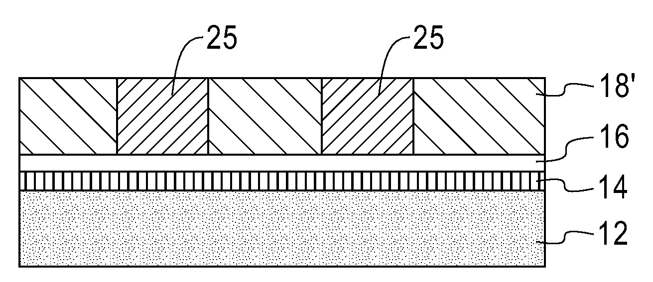
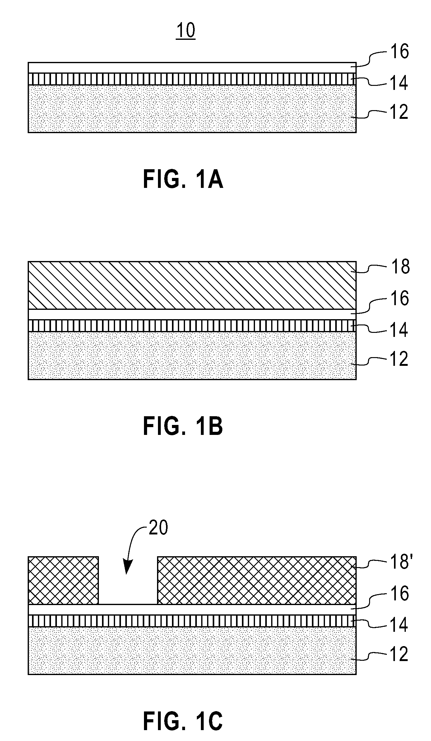
[0160]Single-Damascene Integration of Negative-Tone Patternable Low-K Dielectric Having a Dielectric Constant of 2.7 as an On-Chip Electrical Insulator

A. Material, Composition

[0161]A patternable low-k composition was formulated with 60 g of a 20 wt % solution of 6:4 poly(p-hydroxy-alpha-methylbenzylsilsesquioxane-co-p-alpha-methylbenzylsilsesquioxane) (pHMBS / MBS) in propylene glycol monomethyl ether acetate (PGMEA), 40 g of a 20 wt % solution of the silsesquioxane copolymer LKD-2021, 2 g of a 20 wt % solution of triphenylsulfonium nonaflate in PGMEA, and 2 g of a 0.5 wt % solution of an organic base such as trioctylamine in PGMEA, The resulting patternable low-k formulation was filtered through a 0.2 micron (μm) filter.

B. CVD ARC Process

[0162]A 800 Å silicon carbide (SiC) film was deposited on 350 Å NIBLOK substrate on a 200 mm wafer as an anti-reflective coating. The tool used was a 200 mm CVD tool (Centura) from Applied Materials Inc. The process conditions were as follows: precur...

example 2

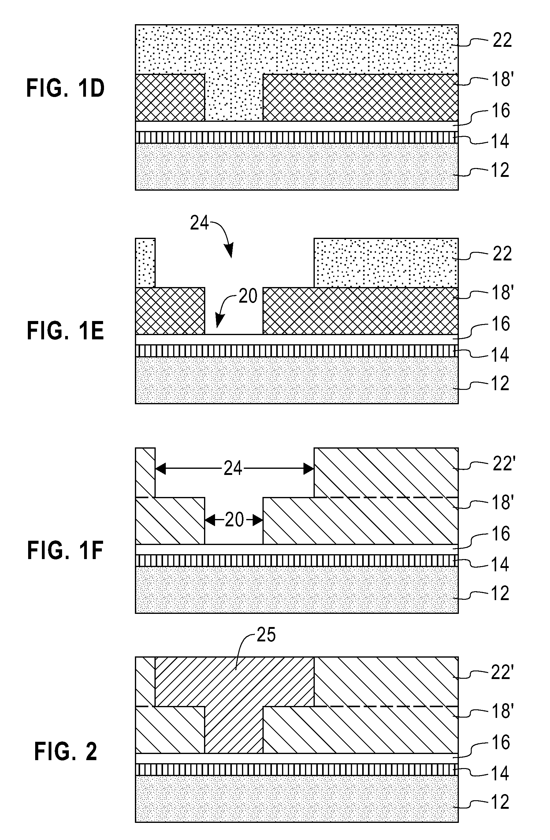
Dual-Damascene Integration of Negative-Tone Patternable Low-K Dielectric Having a Dielectric Constant of 2.7 as an On-Chip Electrical Insulator

A. Material, Composition

[0175]A patternable low-k composition was formulated with 60 g of a 20 wt % solution of 6:4 poly(p-hydroxy-alpha-methylbenzylsilsesquioxane-co-p-alpha-methylbenzylsilsesquioxane) (pHMBS / MBS) in propylene glycol monomethyl ether acetate (PGMEA), 40 g of a 20 wt % solution of the silsesquioxane copolymer LKD-2021, 2 g of a 20 wt % solution of triphenylsulfonium nonaflate in PGMEA, and 2 g of a 0.5 wt % solution of an organic base such as trioctylamine in PGMEA. The resulting patternable low-k formulation was filtered through a 0.2 micron (μm) filter.

B. CVD ARC Process

[0176]A 800 Å silicon carbide (SiC) film was deposited on 350 Å NBLOK substrate on a 200 mm wafer as an anti-reflective coating. The tool used was 200 mm CVD tool (Centura) from Applied Materials Inc. The process conditions are: precursor trimethyl silane (T...


PUM


Abstract

The present invention provides a method of fabricating an interconnect structure in which a patternable low-k material replaces the need for utilizing a separate photoresist and a dielectric material. Specifically, this invention relates to a simplified method of fabricating single-damascene and dual-damascene low-k interconnect structures with at least one patternable low-k dielectric and at least one inorganic antireflective coating. In general terms, a method is provided that includes providing at least one patternable low-k material on a surface of an inorganic antireflective coating that is located atop a substrate, said inorganic antireflective coating is vapor deposited and comprises atoms of M, C and H wherein M is at least one of Si, Ge, B, Sn, Fe, Ta, Ti, Ni, Hf and La; forming at least one interconnect pattern within the at least one patternable low-k material; and curing the at least one patternable low-k material. The inventive method can be used to form dual-damascene interconnect structures as well as single-damascene interconnect structures.

Description

FIELD OF THE INVENTION[0001]The present invention relates to an interconnect structure and a method of fabricating the same. Specifically, the present invention relates to a patternable dielectric film structure and a patternable dielectric interconnect structure with improved lithography. In particular, the invention provides a single-damascene or dual-damascene low-k interconnect structure comprising a patternable dielectric and an antireflective layer deposited from a vapor phase.BACKGROUND OF THE INVENTION[0002]It is widely known that the speed of propagation of interconnect signals is one of the most important factors controlling overall circuit speed as feature sizes are reduced and the number of devices per unit area as well as the number of interconnect levels are increased. Throughout the semiconductor industry, there has been a strong drive to increase the aspect ratio (i.e., height to width ratio) and to reduce the dielectric constant, k, of the interlayer dielectric (ILD...

Claims


Application Information

Patent Timeline
IPC IPC(8): H01L23/52H01L21/4763
CPCH01L21/02118H01L2924/12044H01L21/02274H01L21/02282H01L21/0276H01L21/31H01L21/3121H01L21/3122H01L21/3148H01L21/76808H01L21/76832H01L21/76835H01L21/76843H01L23/53238H01L23/5329H01L23/53295H01L2221/1031H01L21/02167H01L2924/0002H01L2924/00
Inventor LIN, QINGHUANGNEUMAYER, DEBORAH A.
Owner TAIWAN SEMICON MFG CO LTD
Why Eureka
Try Eureka