Semiconductor device
a semiconductor device and semiconductor technology, applied in semiconductor devices, digital storage, instruments, etc., can solve the problems of increasing manufacturing process steps and increasing manufacturing costs, and achieve the effect of reducing the chip area of a semiconductor device having a nonvolatile memory
- Summary
- Abstract
- Description
- Claims
- Application Information
AI Technical Summary
Benefits of technology
Problems solved by technology
Method used
Image

Examples
embodiment 1
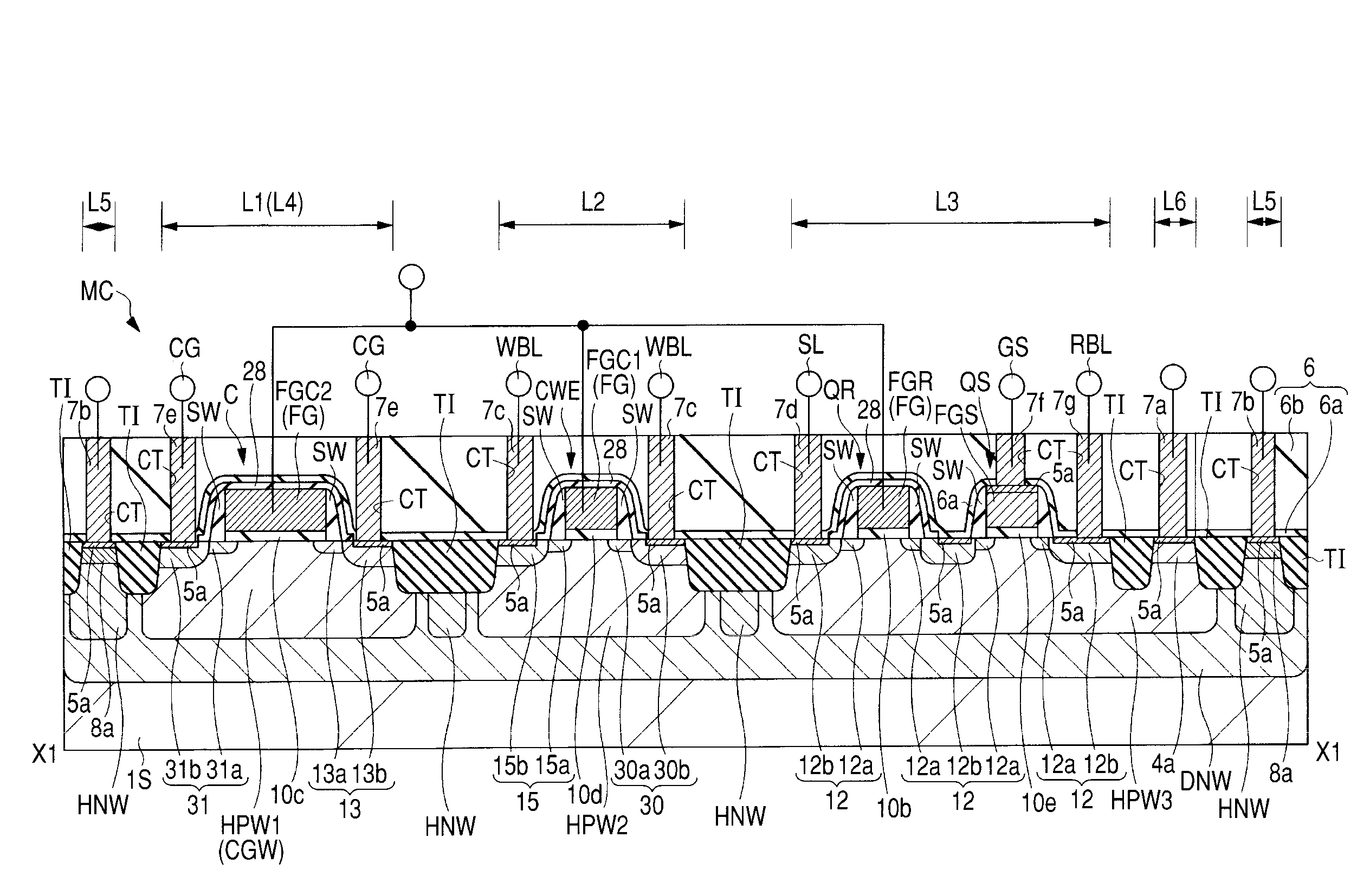
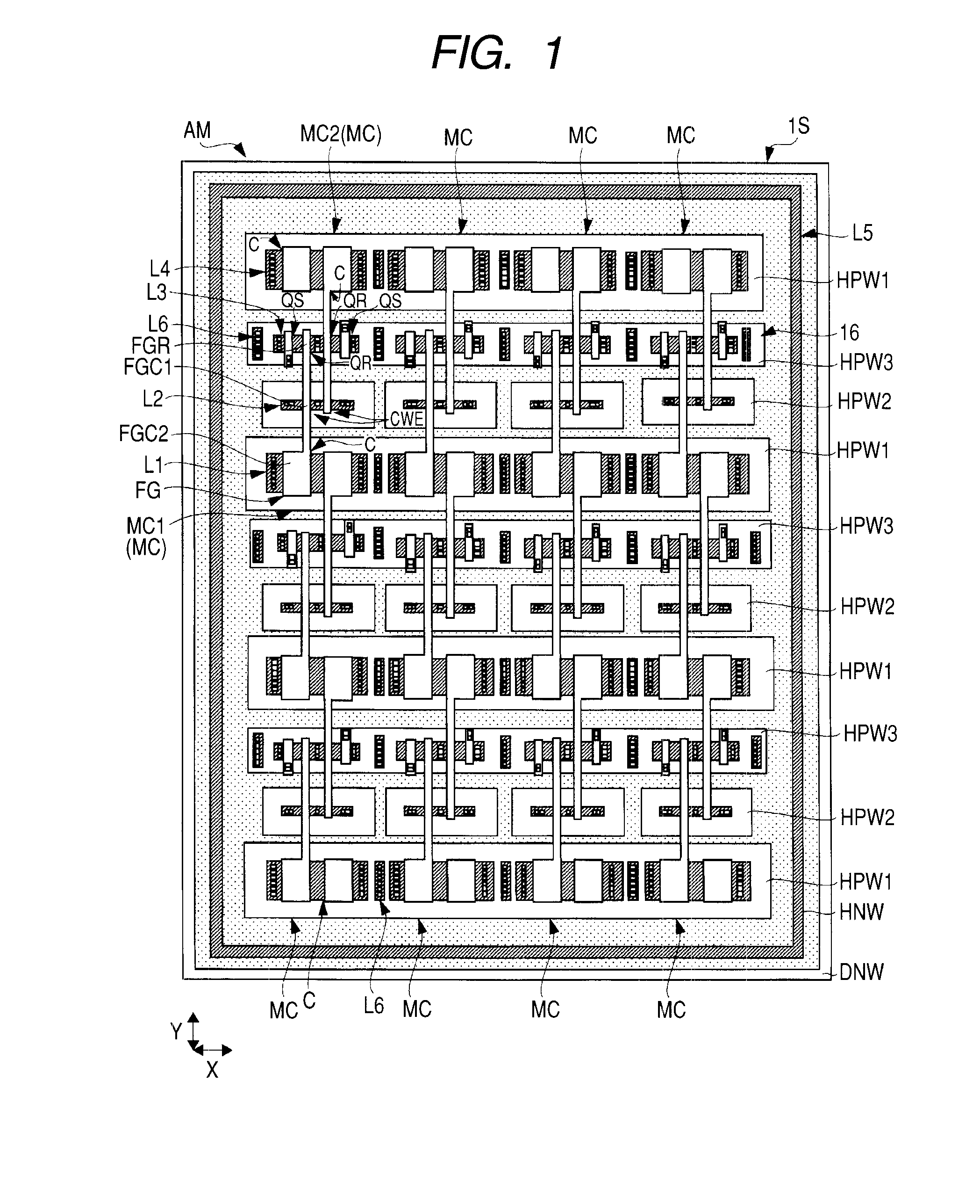
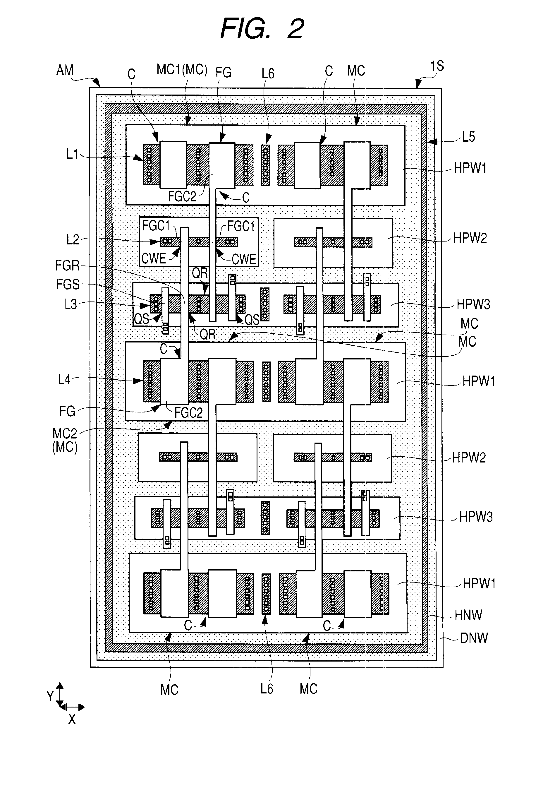
[0054]In a semiconductor device according to a first embodiment of the present invention, a main circuit and a nonvolatile memory for storing desired data (information) of a relatively small capacity related to the main circuit are formed respectively in a main circuit region and a nonvolatile memory region, which are arranged in the same semiconductor chip (semiconductor substrate). The semiconductor substrate (hereinafter referred to as the “substrate”) configuring the semiconductor chip has a principal surface (element formation surface) formed with the main circuit and the nonvolatile memory, and a back surface opposite to the principal surface. A description will be given hereinbelow of a semiconductor device (LCD driver) in which a nonvolatile memory for storing desired information related to a main circuit is formed on a semiconductor chip formed with an LCD (Liquid Crystal Device) driver circuit as the main circuit. The LCD driver described in the present embodiment indicate...
embodiment 2
[0146]In a semiconductor device according to the second embodiment of the present invention, a main circuit and a nonvolatile memory for storing desired data (information) of a relatively small capacity related to the main circuit are formed respectively in a main circuit region and a nonvolatile memory region which are arranged in the same semiconductor chip (semiconductor substrate), in the same manner as in the first embodiment described above. FIG. 22 is a plan view of a nonvolatile memory arranged in the nonvolatile memory region AM of a substrate 1S according to the present second embodiment, which shows the case where the nonvolatile memory has a 12-bit configuration. The nonvolatile memory (see FIG. 22) according to the present second embodiment is different from the nonvolatile memory (see FIGS. 1 to 3) shown in the first embodiment in plan layout.
[0147]As shown in FIG. 22, the nonvolatile memory according to the present second embodiment comprises a plurality of memory cel...
embodiment 3
[0154]In the first embodiment described above, when a write operation is performed to the selected memory cell MCs, the well HPW1 of the capacitor element C is set to 9 V by applying the control voltage of 9 V to the control gate line CG (word line), and the well HPW2 of the write / erase element CWE is set to −9 V by applying the negative voltage of −9 V to the write / erase bit line WBL (data line), so that the FN tunnel current is generated to perform the write operation.
[0155]FIG. 23 is a layout diagram of a memory array in which a plurality of memory cells MC which are arranged at the positions where word lines (control gate lines CG) and data lines (bit lines WBL) intersect each other are arranged as blocks in a matrix, which shows an example of voltages applied to individual components, and the respective conditions of the individual memory cells when a write operation is performed. The conditions of the individual memory cells MC include a selected condition (memory cells MCs), ...
PUM
 Abstract
Description
Claims
Application Information
 - R&D
- Intellectual Property
- Life Sciences
- Materials
- Tech Scout
- Unparalleled Data Quality
- Higher Quality Content
- 60% Fewer Hallucinations
Browse by: Latest US Patents, China's latest patents, Technical Efficacy Thesaurus, Application Domain, Technology Topic, Popular Technical Reports.
© 2025 PatSnap. All rights reserved.Legal|Privacy policy|Modern Slavery Act Transparency Statement|Sitemap|About US| Contact US: help@patsnap.com