Method of improving oxide growth rate of selective oxidation processes

a selective oxidation and growth rate technology, applied in the field of selective oxidation of composite silicon/metal films, can solve the problems of device inoperative, degraded gate characteristics of the layer, and damage to the gate oxide layer

Active Publication Date: 2009-03-26
APPLIED MATERIALS INC
View PDF40 Cites 42 Cited by
  • Summary
  • Abstract
  • Description
  • Claims
  • Application Information

AI Technical Summary

Benefits of technology

[0013]Further embodiments of the invention provide a method of processing a substrate comprising one or more oxide layers and one or more metal or barrier layers, comprising disposing the substrate in a chamber, introducing a quantity of a hydrogen containing gas and a quantity of an oxygen containing gas into the chamber to create a quantity of a gas ...

Problems solved by technology

Likewise, the gate oxide layer may be damaged by repeated cycles of deposition, etching, and plasma processing typically involved in modern device fabrication.
This damage degrades the gate characteristics of the layer, rendering the device inoperative.
Because oxidizing other regions of the transistor may reduce conductivity and impair the device, oxidizing only certain materials in the device is desired.
For example, oxidizing th...

Method used


Image

  • Method of improving oxide growth rate of selective oxidation processes
  • Method of improving oxide growth rate of selective oxidation processes
  • Method of improving oxide growth rate of selective oxidation processes

Examples


Embodiment Construction

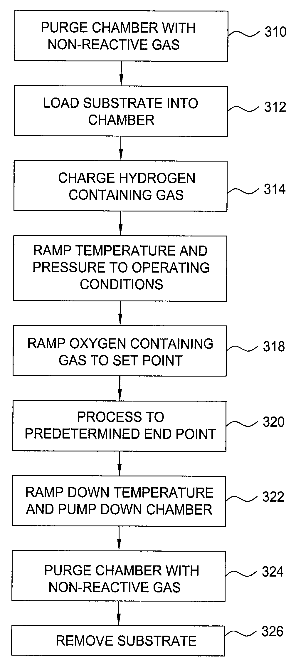
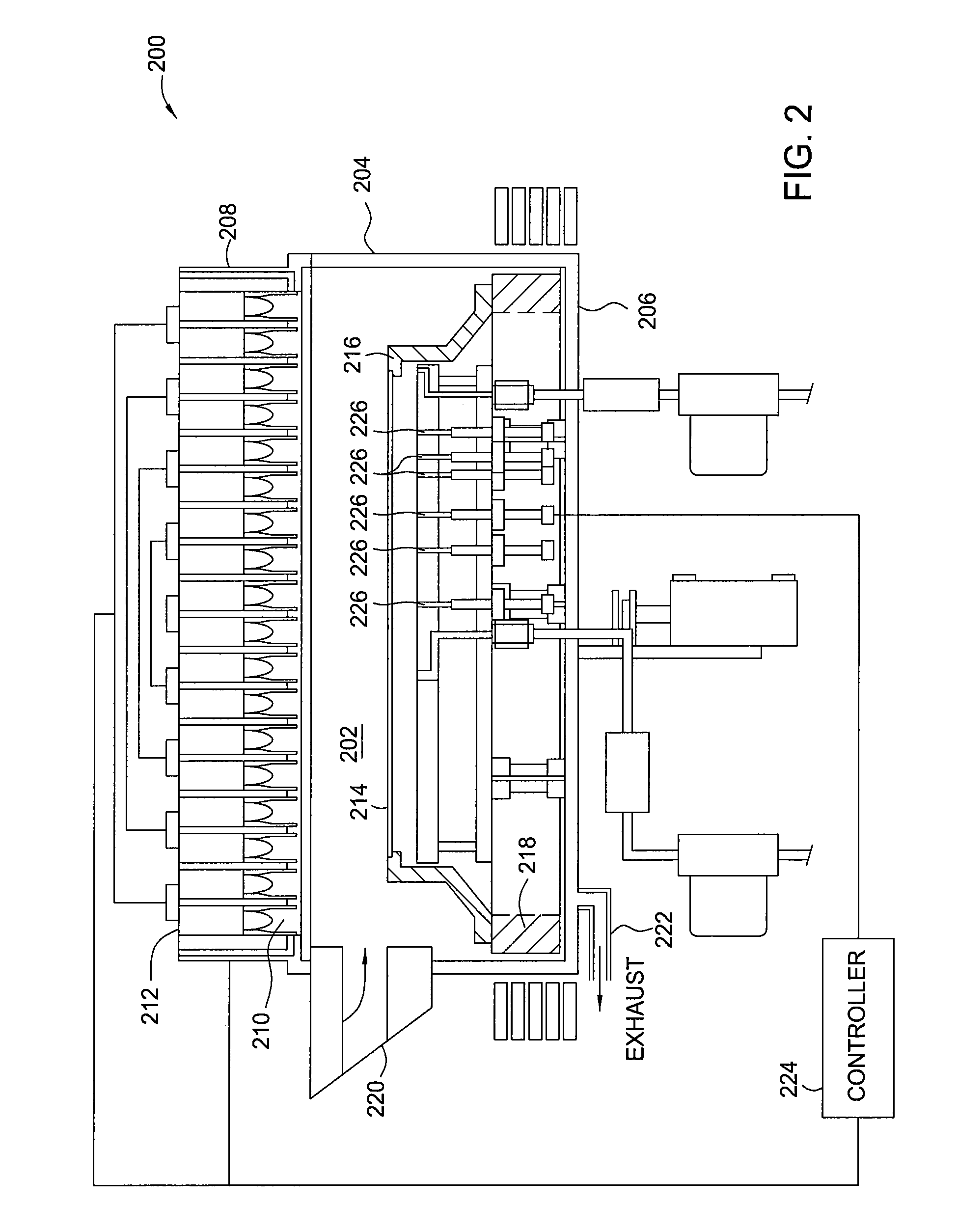
[0026]The present invention describes a method for selectively oxidizing silicon containing materials in a substrate. While the invention will be described below in reference to a rapid thermal heating chamber, such as any of the VANTAGE™ or CENTURA™ devices available from Applied Materials, Inc., of Santa Clara, Calif., it is to be understood that the invention may be practiced in other chambers, including those sold by other manufacturers. FIG. 2 illustrates a rapid thermal heating apparatus 200 that can be used to carry out the process of the present invention. The apparatus features a process chamber 202 that may be evacuated or filled with selected gases, and a side wall 204 and bottom enclosure 206. The upper portion of the sidewall is sealed against a light pipe assembly 208, from which radiant energy is directed into the chamber. The light pipe assembly 208 includes a plurality of tungsten halogen lamps 210, for example Sylvania EYT lamps, each mounted into a light pipe 212 ...


PUM


Abstract

A method for selective oxidation of silicon containing materials in a semiconductor device is disclosed and claimed. In one aspect, a rapid thermal processing apparatus is used to selectively oxidize a substrate by in-situ steam generation at high pressure in a hydrogen rich atmosphere. Other materials, such as metals and barrier layers, in the substrate are not oxidized.

Description

BACKGROUND OF THE INVENTION[0001]1. Field of the Invention[0002]Embodiments of the present invention generally relate to the field of semiconductor manufacturing and more specifically to a method and apparatus for the selective oxidation of a composite silicon / metal film.[0003]2. Description of the Related Art[0004]In the manufacture of semiconductor devices, oxidation of silicon containing substrates plays a key role. For example, in a standard semiconductor device, a gate oxide layer is ordinarily situated over a substrate containing a source region, a drain region, and an intervening silicon or polysilicon region. Metal contacts are deposited over the source and drain regions, and a conductive layer deposited over the gate oxide. The entire structure is often depicted as a stack of layers. When a voltage is applied across the gate oxide generating an electric field oriented along an axis from the substrate, through the gate oxide, to the conductive layer, the electrical character...

Claims


Application Information

Patent Timeline
IPC IPC(8): H01L21/316
CPCH01L21/0223H01L21/02238H01L21/32H01L21/28247H01L21/31662H01L21/02255H01L21/02H01L21/283H01L21/31
Inventor YOKOTA, YOSHITAKATAM, NORMANRAMACHANDRAN, BALASUBRAMANIANRIPLEY, MARTIN JOHN
Owner APPLIED MATERIALS INC
Why Eureka
Try Eureka