Method for inspecting and measuring sample and scanning electron microscope

a scanning electron microscope and sample technology, applied in the field of scanning electron microscope, can solve the problems of inability to detect harmful effects, inability to stabilize charges, and inability to accurately detect the effects of a single sample, so as to speed up observation speed, quick stabilization of charges, and high accuracy

Active Publication Date: 2009-04-02
HITACHI HIGH-TECH CORP
View PDF8 Cites 40 Cited by
  • Summary
  • Abstract
  • Description
  • Claims
  • Application Information

AI Technical Summary

Benefits of technology

[0025]According to such technique and configuration, pre-dose is performed using an electron beam with a beam diameter larger than that of the second electron beam, therefore variation of charge originated to existence of the region not irradiated by a beam can be inhibited. The second electron beam is the electron beam for inspection and measurement, and it should be extremely narrowed to improve the spatial resolution of the device. On the other hand, if the electron beam is narrowed in pre-dose, the region not irradiated by a beam is enlarged as described above. Accordingly, by enlarging the beam diameter of the electron beam in pre-dose compared with the beam for observation and the like, the region not irradiated by a beam described above can be reduced or eliminated, which enables inhibiting of variation of charge in pre-dose.
[0028]Further, as further other aspect applying the pre-dose technology, by shiftingly forming the charge region with respect to the observation region, oblique irradiation of an electron beam becomes possible.
[0029]According to one aspect described above, quick stabilizing of the charge in pre-dose becomes possible, and as a result, realization of speeding-up of observation and the like becomes possible. Also, according to another aspect described above, realization of high accuracy measurement based on uniformed charge within the electron beam scanning region becomes possible. Further, according to further other aspect described above applying the pre-dose technology, realization of observation by an oblique beam becomes possible while inhibiting an aberration formed by a lens.

Problems solved by technology

However, if the irradiation region is enlarged, there is a problem that it takes substantially long time before the charge is stabilized.
If the number of scanning lines remains unchanged, the larger the irradiated region of an electron beam, the larger the non-irradiated region, and its harmful effect becomes conspicuous.
Accordingly, as the electron density of the electron beam lowers, the time required until the charge is stabilized inevitably becomes longer.
Further, because the electric potential is different between the center of pre-dose region and the peripheral part and the potential gradient is formed, drift of the electron beam may possibly occur.

Method used


Image

  • Method for inspecting and measuring sample and scanning electron microscope
  • Method for inspecting and measuring sample and scanning electron microscope
  • Method for inspecting and measuring sample and scanning electron microscope

Examples


Embodiment Construction

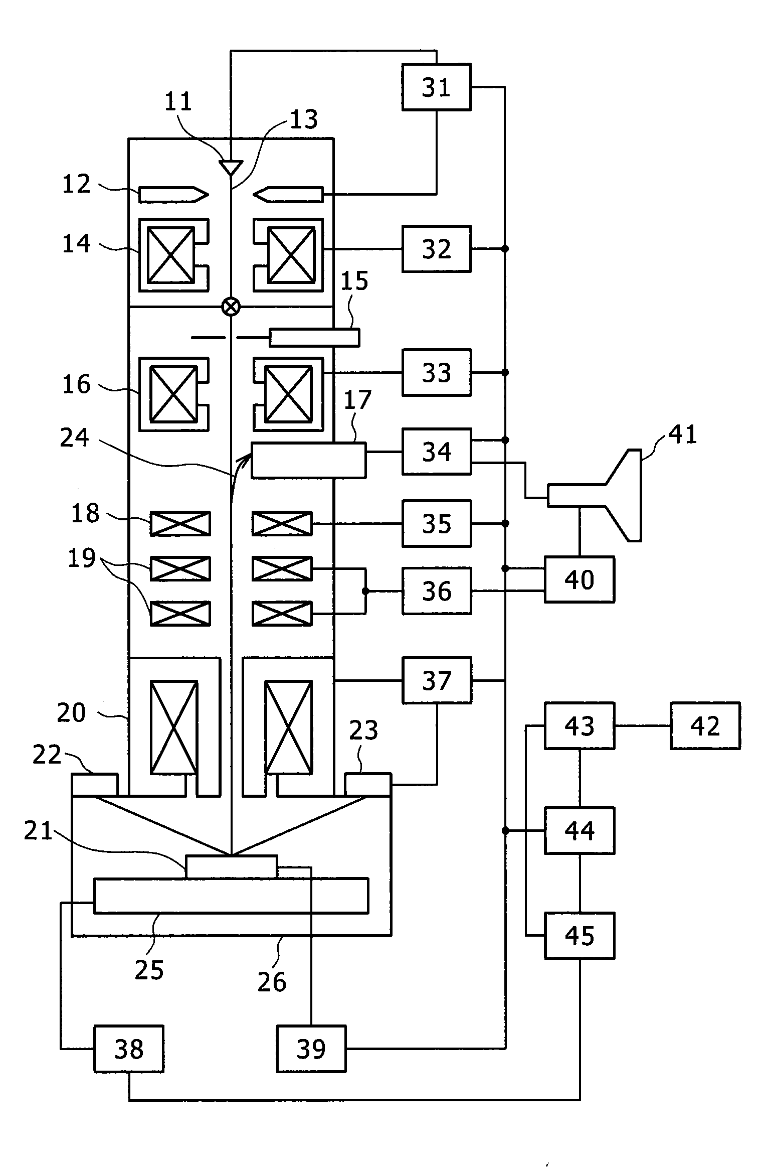
[0053]In the description below, mainly in pre-dose, acceleration voltage is changed to the same with higher secondary electron generation efficiency, and a half band width of an electron beam irradiated interlocking with the area of the preliminary irradiation region is changed. Thus, high charge voltage can be formed on a wafer and the electron beam is irradiated to an entire area of the irradiation region, therefore provision of a method and a device capable of forming the charge effectively becomes possible.

[0054]Also, a method and a device is described wherein, preliminary irradiation is performed by different acceleration voltage after formation of charge, leveling of the charge formed on the surface of a wafer is performed, thereby leveling of the electric field in the vicinity of the wafer formed by the charge voltage becomes possible, and the electric field component in the direction perpendicular to the light axis of the electron beam can be decreased. Thus, even if the pot...


PUM

PropertyMeasurementUnit
aspect ratioaaaaaaaaaa
aperture diameteraaaaaaaaaa

Abstract

As an aspect for realizing accurate observation, inspection, or measurement of the contact hole with large aspect ratio, a method and a device to scan a second electron beam after scanning a first electron beam to a sample to charge the sample are proposed wherein the beam diameter of the first electron beam is made larger than the beam diameter of the second electron beam.

Description

BACKGROUND OF THE INVENTION[0001]The present invention relates to a scanning electron microscope for inspecting and measuring a sample by scanning an electron beam to the sample, particularly to a method and a scanning electron microscope for inspecting and measuring a sample by scanning an electron beam to a sample, charging the sample, and scanning another electron beam to the sample under a charged state.[0002]In recent years, in the light of high integration and micronization of a semiconductor element, a variety of patterns are formed on a sample (a semiconductor wafer, for example), and evaluation and measurement of their shape and size are becoming important more and more.[0003]Particularly, in a contact hole for obtaining electric conduction between layers in multilayering, the diameter of the hole is becoming minute as micronization proceeds, and a contact hole with an aspect ratio (depth of contact hole / diameter of hole) of over 30 is not uncommon at present.[0004]To obser...

Claims


Application Information

Patent Timeline
Patent Type & Authority Applications(United States)
IPC IPC(8): G01N23/00
CPCG01N23/2251H01J37/265H01J37/26H01J2237/0048H01J2237/281H01J37/28
Inventor EZUMI, MAKOTOIWAMA, SATORUKAKUTA, JUNICHISATO, TAKAHIROIKEGAMI, AKIRA
Owner HITACHI HIGH-TECH CORP
Why Eureka
Try Eureka