Semiconductor storage device

Inactive Publication Date: 2009-04-02
RENESAS ELECTRONICS CORP
View PDF2 Cites 9 Cited by
  • Summary
  • Abstract
  • Description
  • Claims
  • Application Information

AI Technical Summary

Benefits of technology

[0018]According to the semiconductor storage device of the present invention, the other potential of the source or the drain of the third transistor is fixed to a fixed potential in the memory cell non-selected state. Accordingly, it is possible to prevent the potential of the other terminal of the source or the drain of the third transistor from being

Problems solved by technology

However, transistors forming the SRAM cell have been miniaturized in recent years and the current driving ability of the transistor has been decreasing, which interrupts the high-speed operation.
However, the nMOS transistor Tr40 has a large channel leak current as well.
Therefore, when the potential of the high level reduces in the bit line, a sense amplifier may falsely detect the potential difference of the bit line pair, which causes the data reading failure.
Further, since

Method used


Image

  • Semiconductor storage device
  • Semiconductor storage device
  • Semiconductor storage device

Examples


Embodiment Construction

[0032]The invention will now be described herein with reference to illustrative embodiments. Those skilled in the art will recognize that many alternative embodiments can be accomplished using the teachings of the present invention and that the invention is not limited to the embodiments illustrated for explanatory purposes.

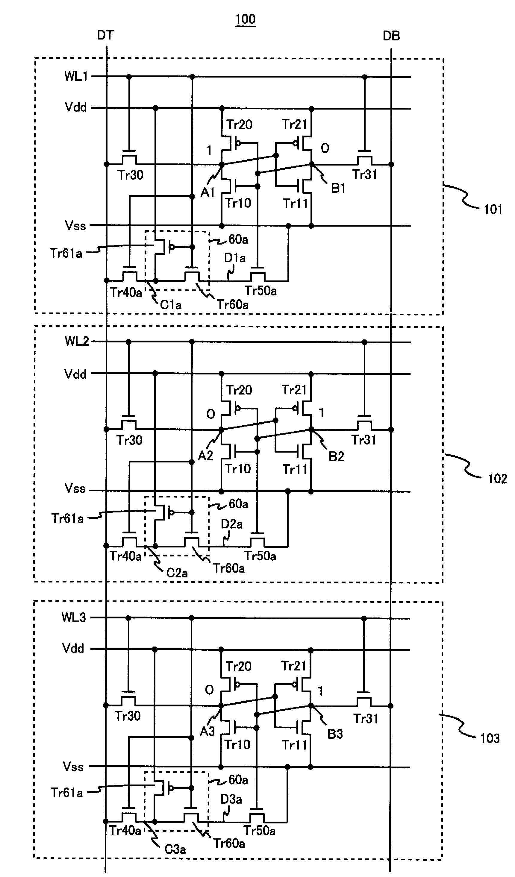
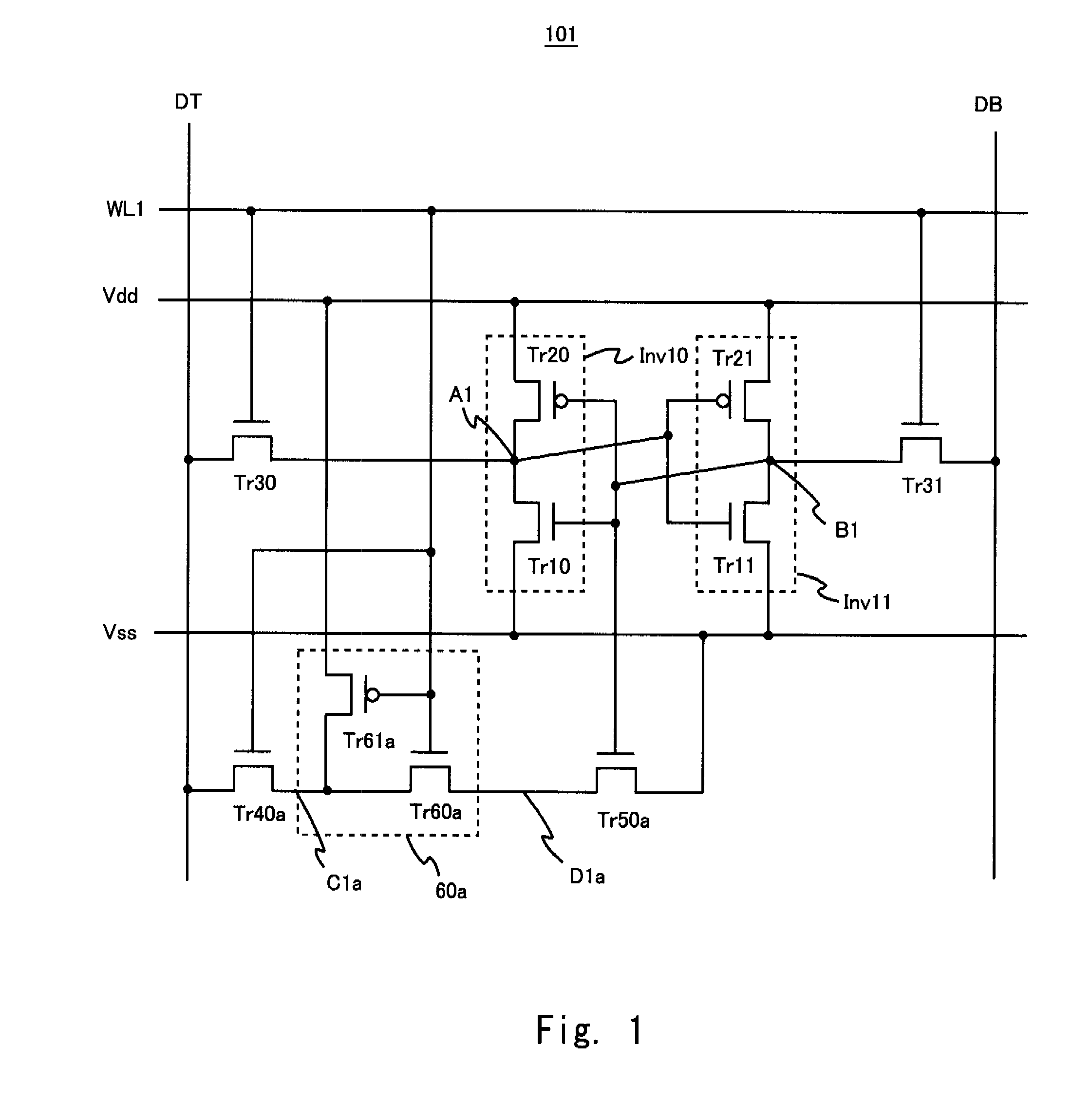
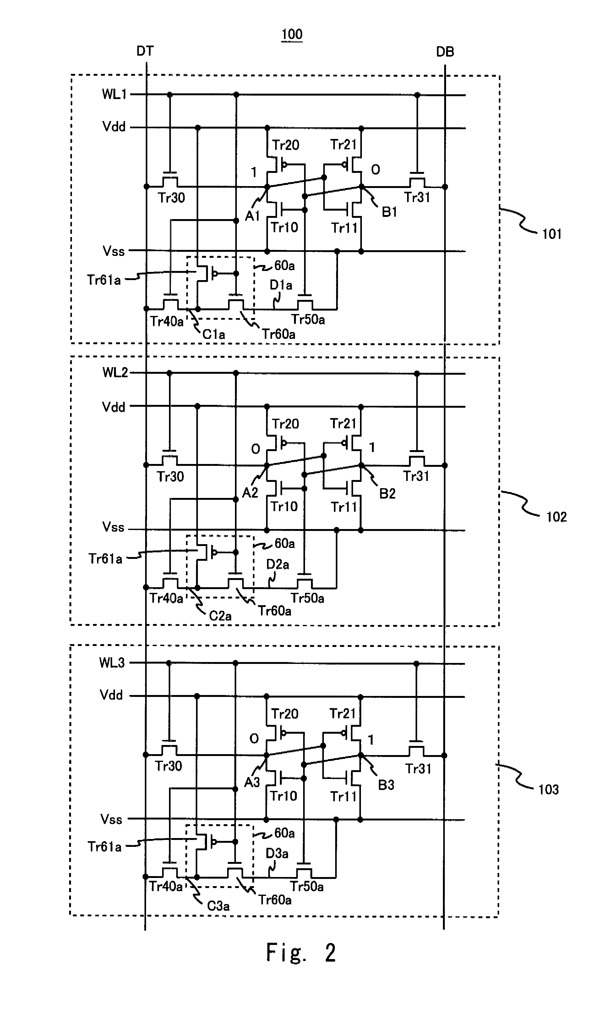
[0033]The specific embodiment to which the present invention is applied will now be described in detail with reference to the drawings. This embodiment is the one in which the present invention is applied to an SRAM.

[0034]FIG. 1 shows one example of a circuit configuration of a memory cell of a semiconductor storage device of the present embodiment. As shown in FIG. 1, a memory cell 101 includes a bit line pair including a bit line DT (first bit line) and a bit line DB (second bit line), an inverter Inv10 (first inverter), an inverter Inv11 (second inverter), an nMOS transistor Tr30 (first transistor), and an nMOS transistor Tr31 (second transistor).

[0035]An outp...


PUM


Abstract

In a semiconductor storage device including a transistor for reading port, undesired voltage decrease may occur in a bit line in a reading operation due to a leak current from the transistor for reading port of a memory cell, which may cause a reading error. A semiconductor storage device according to one aspect of the present invention includes a third transistor having one of a source and a drain connected to a first bit line and switching supply of a ground voltage performed on the first bit line in accordance with a value held in a memory cell according to selection and non-selection of the memory cell, and a fixed voltage keeping circuit keeping a potential of the other of the source and the drain of the third transistor to a fixed potential in a memory cell non-selected state in a six-transistor SRAM.

Description

BACKGROUND OF THE INVENTION[0001]1. Field of the Invention[0002]The present invention relates to a semiconductor storage device.[0003]2. Description of Related Art[0004]An electronic device such as a computer typically includes a data storing means storing data. One of semiconductor storage devices employed as the data storing means includes an SRAM (Static Random Access Memory). The SRAM has the advantage of high-speed operation that there is no need to perform a refresh operation and that the memory cell access time is short and so on.[0005]However, transistors forming the SRAM cell have been miniaturized in recent years and the current driving ability of the transistor has been decreasing, which interrupts the high-speed operation. In order to facilitate the data reading operation of the memory cell, there has been proposed an SRAM driving bit lines by a read-only transistor having high driving ability. One example of the SRAM including the read-only transistor is disclosed in Ja...

Claims


Application Information

Patent Timeline
IPC IPC(8): G11C11/00G11C7/00
CPCG11C11/412
Inventor ASAYAMA, SHINOBU
Owner RENESAS ELECTRONICS CORP
Why Eureka
Try Eureka