Resistor and fet formed from the metal portion of a mosfet metal gate stack

a metal gate stack and resistor technology, applied in the field of polysilicon resistor fabrication, can solve the problems of reducing the time propagation delay rc of the gate, and reducing the effective gate capacitance of the metal insulator semiconductor device, etc., to achieve excellent resistor tolerance and no additional cost

Active Publication Date: 2009-04-09
TWITTER INC
View PDF4 Cites 104 Cited by
  • Summary
  • Abstract
  • Description
  • Claims
  • Application Information

AI Technical Summary

Benefits of technology

[0009]An advantage of the method and the resulting structure is that the metal layer thickness is tightly controlled thereby providing an excellent resistor tolerance. The metal layer thickness naturally provides for a suitable resistor sheet resistance value of between 50-300 Ω / square.
[0010]Another advantage is that the resistor formed by the metal layer within the gate electrode stack will be on the same chip as MOSFETs fabricated with HiK metal gate stack and will have no additional cost.

Problems solved by technology

A disadvantage of utilizing polysilicon gates is that at inversion, polysilicon gate electrodes generally experience depletion of carriers in the area of the polysilicon gate adjacent to the gate dielectric.
Such depletion of carriers, which is referred to in the art as the polysilicon depletion effect, reduces the effective gate capacitance of the Metal Insulator Semiconductor (MIS) device.
The decrease in resistance causes a decrease in the time propagation delay RC of the gate.
Although a silicide top gate region may help to decrease the resistance of the transistor, charge is still depleted in the vicinity of the interface formed between the bottom polysilicon gate and gate dielectric, thereby causing a smaller effective gate capacitance.
This approach can have drawbacks due to the multiple process steps that influence the resistance value, and thus increase resistor tolerance.
This adds significant process costs to the technology due to additional deposition, lithography and etching steps.

Method used


Image

  • Resistor and fet formed from the metal portion of a mosfet metal gate stack
  • Resistor and fet formed from the metal portion of a mosfet metal gate stack
  • Resistor and fet formed from the metal portion of a mosfet metal gate stack

Examples


Embodiment Construction

[0026]Step A

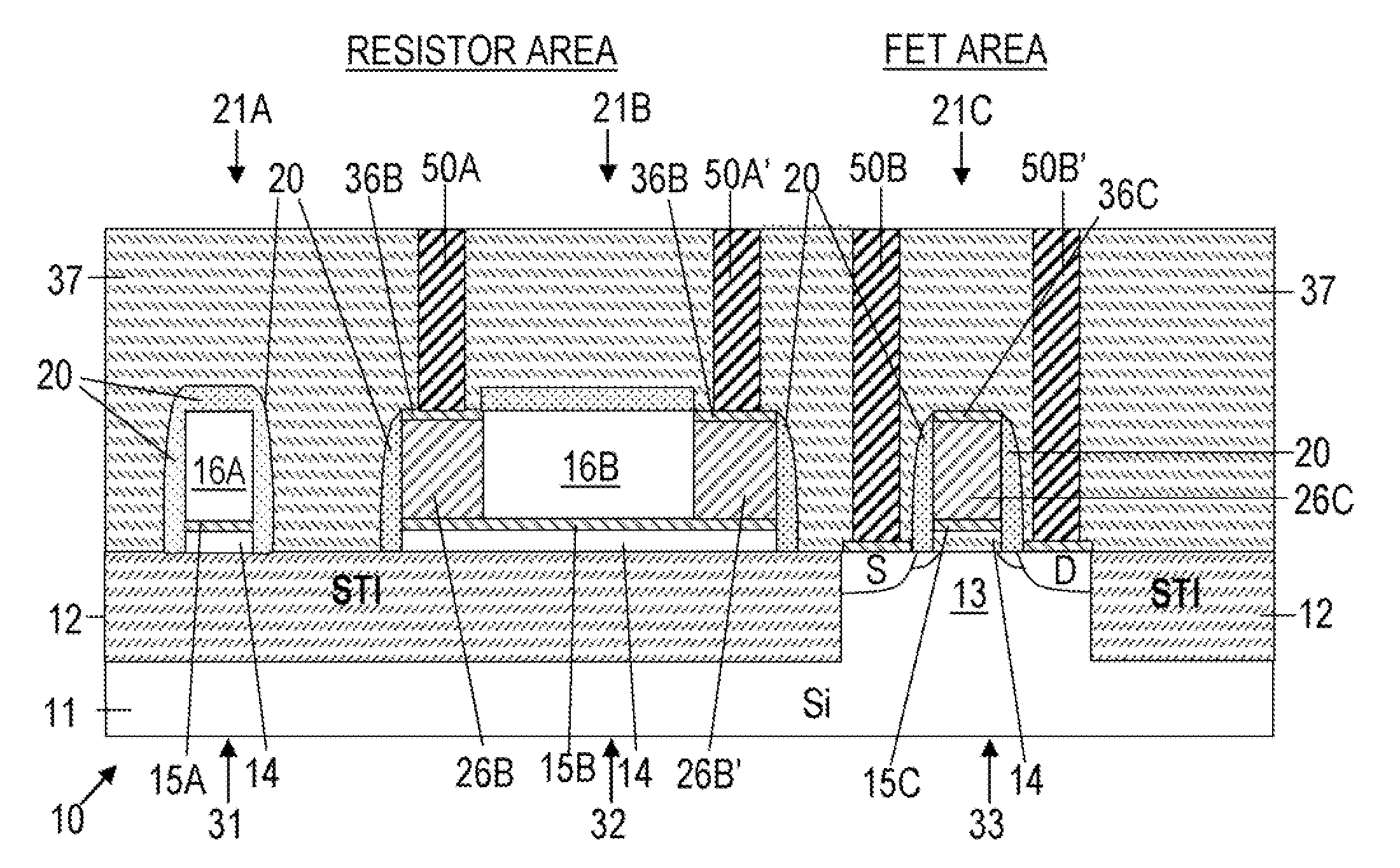
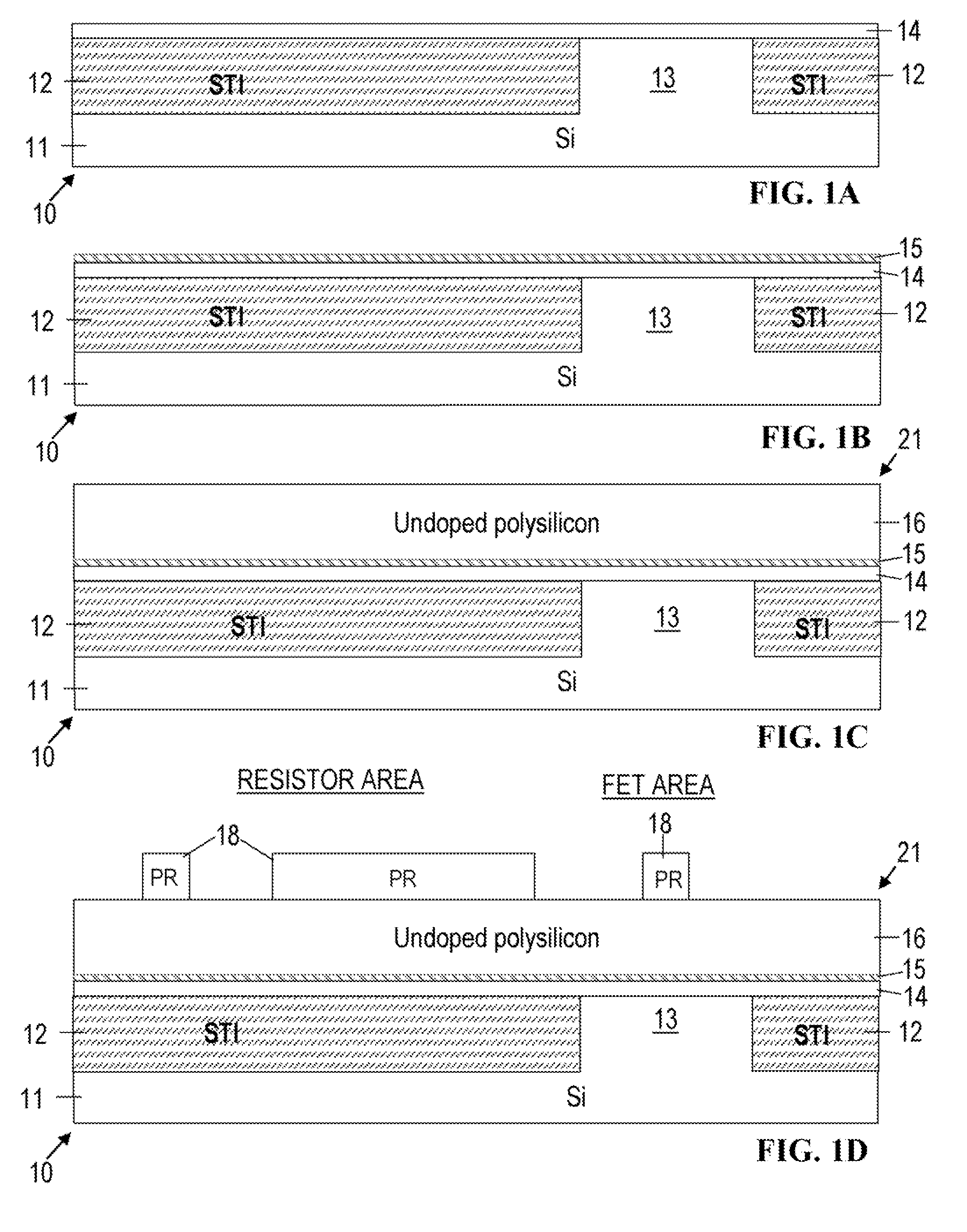
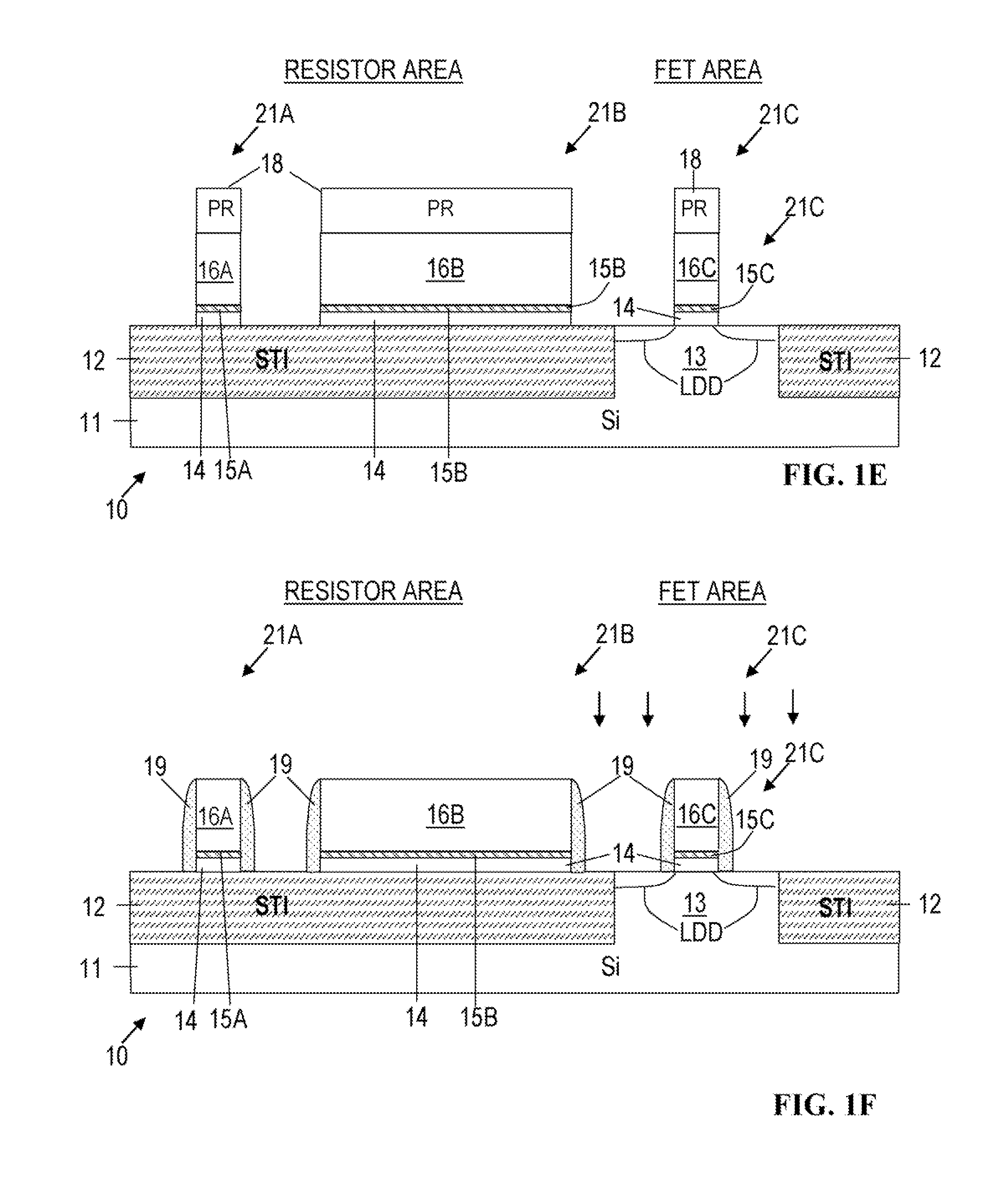
[0027]FIG. 1A shows a device 10 in an early stage of manufacture with a silicon semiconductor substrate 11. The substrate 11 may comprise a Silicon-On-Insulator (SOI) substrate or other known substrates which can support fabrication of integrated circuits. Between the STI regions 12 a source / drain / channel region 13 is defined in the silicon substrate 11. In order to produce the device 10 of FIG. 1A, a set of well known conventional processing steps employed in the early stages of fabrication of Complementary Metal Insulator Semiconductor (CMIS) Field Effect Transistor (FET) devices are performed including formation of a pair of Shallow Trench Isolation (STI) regions 12, formation of N wells and P wells, threshold adjustment implantation, all of which steps are well known by those skilled in the art.

[0028]A blanket insulator layer 14 has been thermally grown or deposited, over the surface of The device 10. Alternatively, any combination of these materials may be formed as...


PUM


Abstract

An integrated semiconductor device includes a resistor and an FET device formed from a stack of layers. The stack of layers includes a dielectric layer formed on a substrate; a metal conductor layer having lower electrical resistance formed on the dielectric layer; and a polysilicon layer formed on the metal conductor layer. A resistor stack is formed by patterning a portion of the original stack of layers into a resistor. An FET stack is formed from another portion of the original stack of layers. The FET stack is doped to form a gate electrode and the resistor stack is doped aside from the resistor portion thereof. Then terminals are formed at distal ends of the resistor in a doped portion of the polysilicon layer. Alternatively, the polysilicon layer is etched away from the resistor stack followed by forming terminals at distal ends of the metal conductor in the resistor stack.

Description

BACKGROUND OF THE INVENTION[0001]The present invention relates to semiconductor devices and more particularly to a process for fabricating polysilicon resistors for use in integrated circuits including Field Effect Transistor (FET) devices.[0002]Heretofore, in the case of Complementary Metal Insulator Semiconductor (CMIS) Complementary Metal Oxide Semiconductor (CMOS) (FET) technology, it has been typical for the gate electrode stack of a Metal Oxide (MOS) FET device to comprise a conductor in the form of a doped polysilicon gate electrode formed over a gate dielectric layer composed of a dielectric material such as silicon oxide. A disadvantage of utilizing polysilicon gates is that at inversion, polysilicon gate electrodes generally experience depletion of carriers in the area of the polysilicon gate adjacent to the gate dielectric. Such depletion of carriers, which is referred to in the art as the polysilicon depletion effect, reduces the effective gate capacitance of the Metal I...

Claims


Application Information

Patent Timeline
Patent Type & Authority Applications(United States)
IPC IPC(8): H01L29/78H01L21/20
CPCH01L21/28088H01L27/0629H01L29/7833H01L29/4966H01L29/6659H01L28/20
Inventor FREEMAN, GREGORY G.HENSON, WILLIAM K.
Owner TWITTER INC
Why Eureka
Try Eureka