
Semiconductor package having marking layer

a technology of semiconductor packages and markings, applied in the direction of semiconductor devices, semiconductor/solid-state device details, electrical apparatus, etc., can solve the problems of high risk of scribing laser beam digging through grooves, and inability to meet the requirements of stacking, so as to maintain the flatness of the device top surface, the effect of precious thinness of semiconductor packages and the suitability for stacking

Active Publication Date: 2009-04-09
TEXAS INSTR INC
View PDF12 Cites 8 Cited by
  • Summary
  • Abstract
  • Description
  • Claims
  • Application Information

AI Technical Summary

Benefits of technology

[0014]It is a technical advantage of the invention that the thin sheet on the device top surface uses compounds undergoing color and reflection changes instead of evaporating or sputtering after absorbing impinging laser pulses. As a consequence, the package top surface remains flat and free of debris and damage by grooves, which in known technology represent a risk for exposing surface-near wire arches.
[0015]It is a technical advantage that the invention maintains the flatness of the device top surface because the symbol-inscribing method of the invention avoids the deposition of ink, which typically heaps ink material on the surface, and the drilling of grooves with pile-up of debris caused by laser marking. As a consequence, the precious thinness of semiconductor packages and suitability for stacking are fully maintained.
[0016]It is another technical advantage of the invention that the method of symbolization is applicable for batch processing and chip-scale packages. The device singulation step can thus be performed as the last step before shipping.

Problems solved by technology

Whenever the bonding wire tops come in close proximity to the package top surface, there is a high risk that the scribing laser beam digs the grooves all the way through the thin encapsulation material to expose the bond wire arch tops.
When this damage happens, the device becomes useless.
Consequently, the conventional method of incorporating the device symbolization for packaged wire-bonded chips into the surface of the package compound may result in unacceptable failure rates for ultra-thin devices.

Method used


Image

  • Semiconductor package having marking layer
  • Semiconductor package having marking layer
  • Semiconductor package having marking layer

Examples


Embodiment Construction

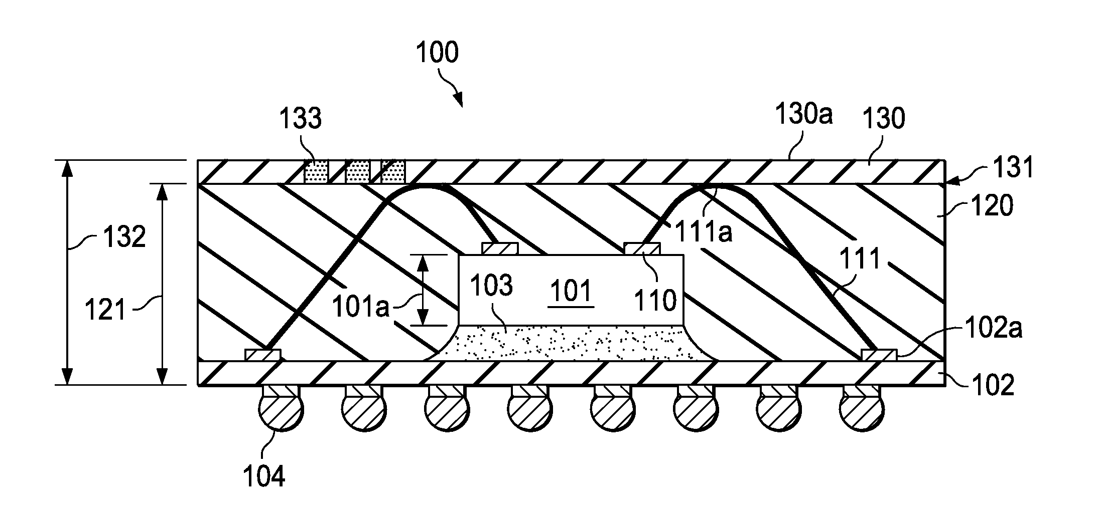
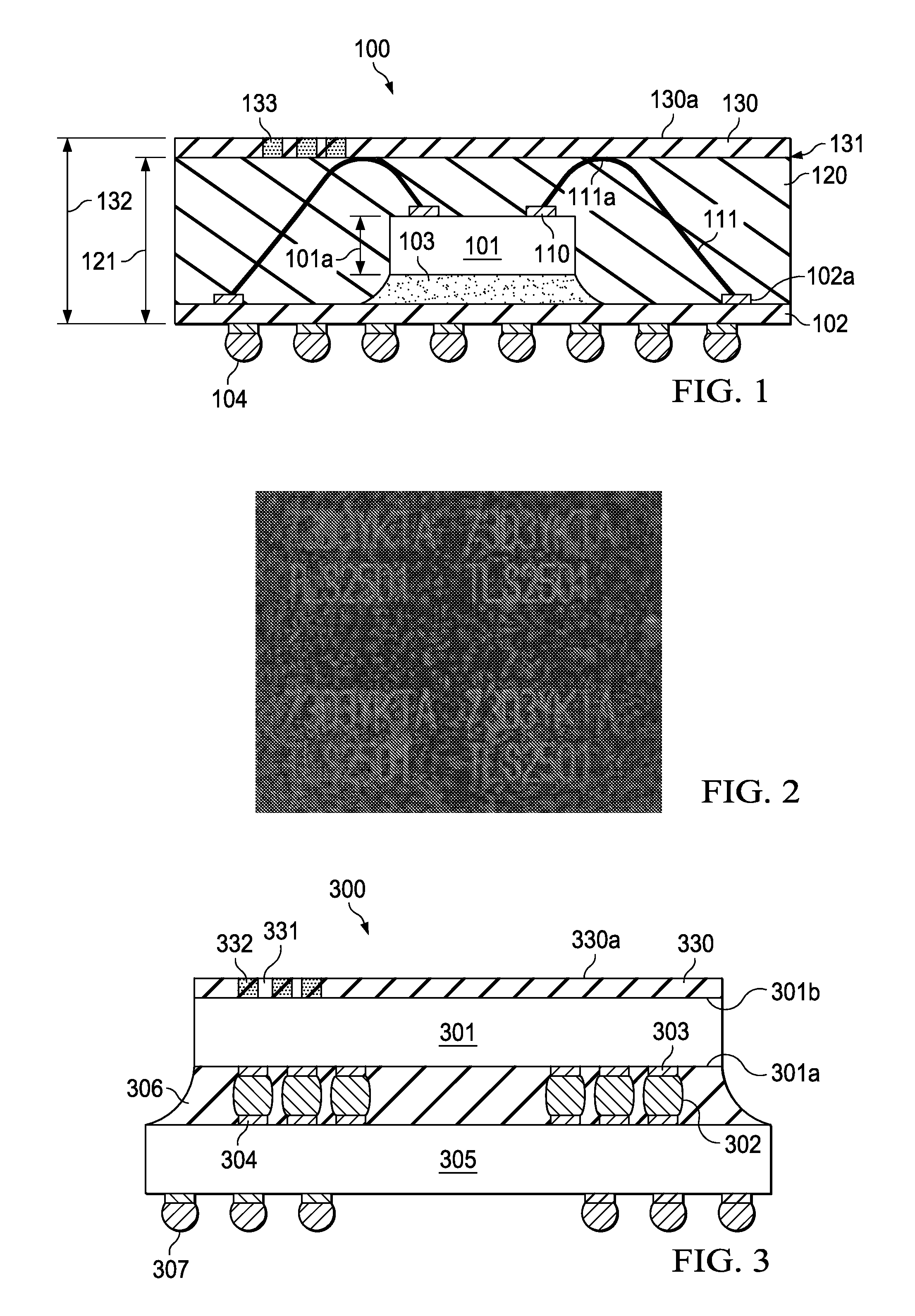
[0028]FIG. 1 shows a semiconductor device generally designated 100 as an embodiment of the invention. An assembled semiconductor chip 101 is encapsulated in a polymeric compound 120. On the top surface of compound 120 is a sheet 130, preferably made of a polymeric material (see below), attached to and in contiguous contact with the compound of encapsulation 120. Sheet 130 has a surface 130a, which is bare and substantially flat. As FIG. 1 indicates, the encapsulation compound and sheet 130 share a border 131.

[0029]The polymeric material of sheet 130 is selected to provide the sheet with a first optical reflectivity and a first color. When an energy pulse such as the pulse of focused laser light, or another high intensity light source, is shining on a spot 133 of sheet 130, the energy is absorbed by the material of the spot, predominantly as thermal energy, elevating the temperature of the spot. The polymeric material alters its chemical configuration locally so that the modified mat...


PUM


Abstract

The symbolization of a semiconductor device (100) is incorporated in a thin sheet (130) attached to the top of the device, facing outwardly with its bare surface. The material of the sheet (about 1 to 10 μm thick) includes regions of a first optical reflectivity and a first color, and regions (133) of a second optical reflectivity and a second color, which differ from, and contrast with, the first reflectivity and color. Preferred choices for the sheet material include the compound o-cresol novolac epoxy and the compound bisphenol-A, more preferably with the chemical imidazole added to the film material. A preferred embodiment of the invention is a packaged device with a semiconductor chip a (101) connected to a substrate (102); the connection is achieved by bonding wires (111) forming an arch with a top 111a. The chip, the wire arches, and the substrate are embedded in an encapsulation material (120), which borders on the attached top sheet so that the arch tops touch the border (131).

Description

RELATED APPLICATIONS[0001]This application claims the benefit of provisional application Ser. Nos. 60 / 977,727, and 60 / 977,731, both filed on Oct. 5, 2007.FIELD OF THE INVENTION[0002]The present invention is related in general to the field of semiconductor devices and processes, and more specifically to the structure and fabrication method of packages with an attached additional sheet selected for marking with pulsed and focused high energy beams.DESCRIPTION OF THE RELATED ART[0003]In the process flow of packaging semiconductor chips into complete devices, typically the last step is the symbolization of the device. This step records the information the user needs to know for proper identification and usage of the device. Examples include device type and model, manufacturer, key performance characteristics, and dates. Typical symbolization elements include, numbers, alphabetic letters, trademark symbols, punctuations, arrows, etc. Among the favorite symbolization techniques are stampi...

Claims


Application Information

Patent Timeline
Patent Type & Authority Applications(United States)
IPC IPC(8): H01L23/544H01L21/56
CPCH01L21/561H01L23/3128H01L23/544H01L24/16H01L24/48H01L24/85H01L24/97H01L2221/68331H01L2223/54406H01L2223/5442H01L2223/54433H01L2223/5448H01L2223/54486H01L2224/2919H01L2224/48091H01L2224/48227H01L2224/73265H01L2224/97H01L2924/01002H01L2924/01029H01L2924/01074H01L2924/01079H01L2924/14H01L2924/15311H01L2924/01006H01L2924/01033H01L2224/16225H01L2224/32225H01L2224/73204H01L24/83H01L2224/85H01L2224/83H01L2924/00014H01L2924/0665H01L2924/07025H01L2924/00H01L2924/00012H01L24/73H01L2924/181H01L2224/45099H01L2224/45015H01L2924/207
Inventor ANO, KAZUAKILEE, WEN YU
Owner TEXAS INSTR INC
Learn More