Light-emitting device, display, and electronic apparatus
a technology of light-emitting devices and electronic devices, which is applied in the direction of discharge tube luminescnet screens, other domestic articles, organic semiconductor devices, etc., can solve the problems of difficult to efficiently inject carriers (electrons and holes) into the light-emitting layers, and achieve the effect of reliable electronic devices
- Summary
- Abstract
- Description
- Claims
- Application Information
AI Technical Summary
Benefits of technology
Problems solved by technology
Method used
Image

Examples
first embodiment
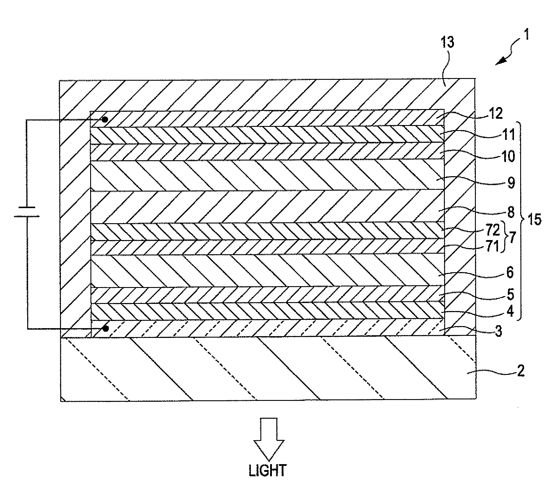
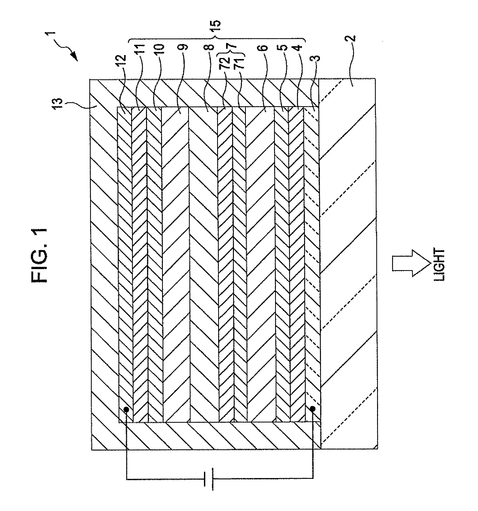
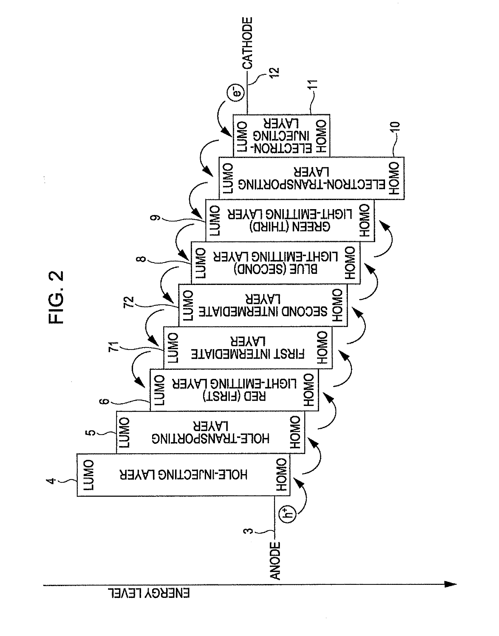
[0064]FIG. 1 is a longitudinal sectional view schematically showing a light-emitting device according to a first embodiment of the invention. FIG. 2 is a diagram illustrating the energy levels of individual layers of the light-emitting device shown in FIG. 1. For convenience of illustration, the top of FIG. 1 is referred to as the “top” of the device, whereas the bottom of FIG. 1 is referred to as the “bottom” of the device.
[0065]Referring to FIG. 1, a light-emitting device (EL device) 1 emits white light by combining red (R) light, green (G) light, and blue (B) light.
[0066]The light-emitting device 1 includes an anode 3, a hole-injecting layer 4, a hole-transporting layer 5, a red light-emitting layer (first light-emitting layer) 6, an intermediate layer 7, a blue light-emitting layer (second light-emitting layer) 8, a green light-emitting layer (third light-emitting layer) 9, an electron-transporting layer 10, an electron-injecting layer 11, and a cathode 12 that are stacked in th...
second embodiment
[0213]FIG. 3 is a longitudinal sectional view schematically showing a light-emitting device according to a second embodiment of the invention. FIG. 4 is a diagram illustrating the energy levels of individual layers of the light-emitting device shown in FIG. 3. For convenience of illustration, the top of FIG. 3 is referred to as the “stop” of the device, whereas the bottom of FIG. 2 is referred to as the “bottom” of the device.
[0214]A light-emitting device 1A according to this embodiment is the same as the light-emitting device 1 according to the first embodiment except that a third intermediate layer is disposed between the first and second intermediate layers.
[0215]In the light-emitting device 1A according to this embodiment, the anode 3, the hole-injecting layer 4, the hole-transporting layer 5, the red light-emitting layer (first light-emitting layer) 6, an intermediate layer 7A, the blue light-emitting layer (second light-emitting layer) 8, the green light-emitting layer (third ...
example 1
[0258](1) First, a transparent glass substrate with an average thickness of 0.5 mm was prepared. An ITO electrode (anode) with an average thickness of 100 nm was formed on the substrate by sputtering.
[0259]The substrate was dipped in ethanol and was subjected to ultrasonic cleaning before the substrate was subjected to oxygen plasma treatment.
[0260](2) Next, a hole-injecting layer with an average thickness of 20 nm was formed on the ITO electrode by vacuum deposition using CuPc.
[0261](3) Next, a hole-transporting layer with an average thickness of 40 nm was formed on the hole-injecting layer by vacuum deposition using α-NPD.
[0262](4) Next, a red light-emitting layer (first light-emitting layer) with an average thickness of 10 m was formed on the hole-transporting layer by vacuum deposition using the material of the red light-emitting layer. The material of the red light-emitting layer contained RD001 (manufactured by Idemitsu Kosan Co., Ltd.) as a red light-emitting material (guest ...
PUM
| Property | Measurement | Unit |
|---|---|---|
| Thickness | aaaaa | aaaaa |
| Thickness | aaaaa | aaaaa |
| Energy level | aaaaa | aaaaa |
Abstract
Description
Claims
Application Information