Roll-on encapsulation method for semiconductor packages

a technology of semiconductor packaging and encapsulation, which is applied in the direction of semiconductor devices, semiconductor/solid-state device details, electrical devices, etc., can solve the problems of high cost of acquiring and maintaining molds, high failure rate, and perennial shortcomings, and achieves low viscosity, high encapsulation productivity, and the effect of eliminating a number of perennial shortcomings

Active Publication Date: 2009-04-09
TEXAS INSTR INC
View PDF7 Cites 18 Cited by
  • Summary
  • Abstract
  • Description
  • Claims
  • Application Information

AI Technical Summary

Benefits of technology

[0015]It is a technical advantage that the invention eliminates a number of perennial shortcomings of the conventional molding technology. Since the method allows the encapsulation not only of a substrate strip, but of whole substrate sheets, the invention lends itself to high encapsulation productivity. Since the deposition of the low viscosity, cream-li

Problems solved by technology

Applicant recognized that today's failure rate of 300 to 600 ppm caused by excess wire sweep during the transfer molding operation for semiconductor packages is unacceptable for the ongoing market trend towards more integrated and miniaturized semiconductor components, especially when this failure rate could get worse due to the introduction of thinner gold wires, driven by co

Method used


Image

  • Roll-on encapsulation method for semiconductor packages
  • Roll-on encapsulation method for semiconductor packages

Examples


Embodiment Construction

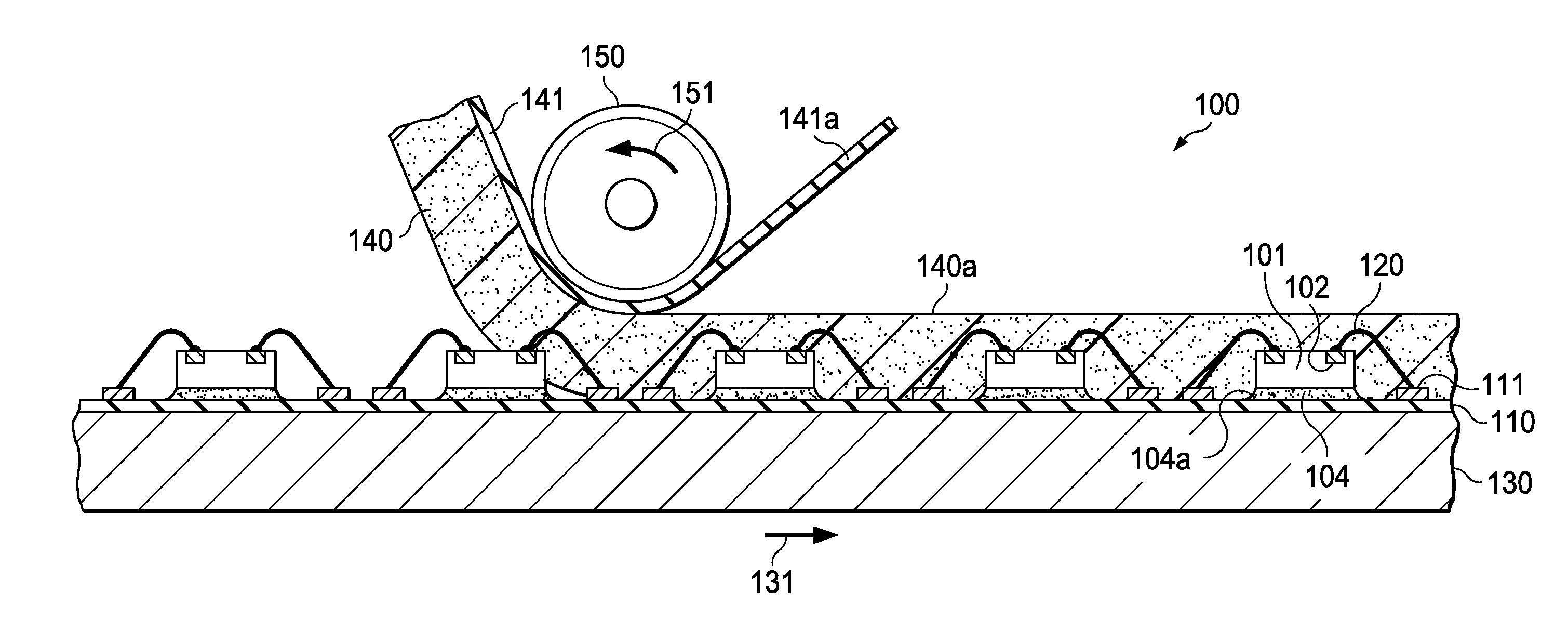
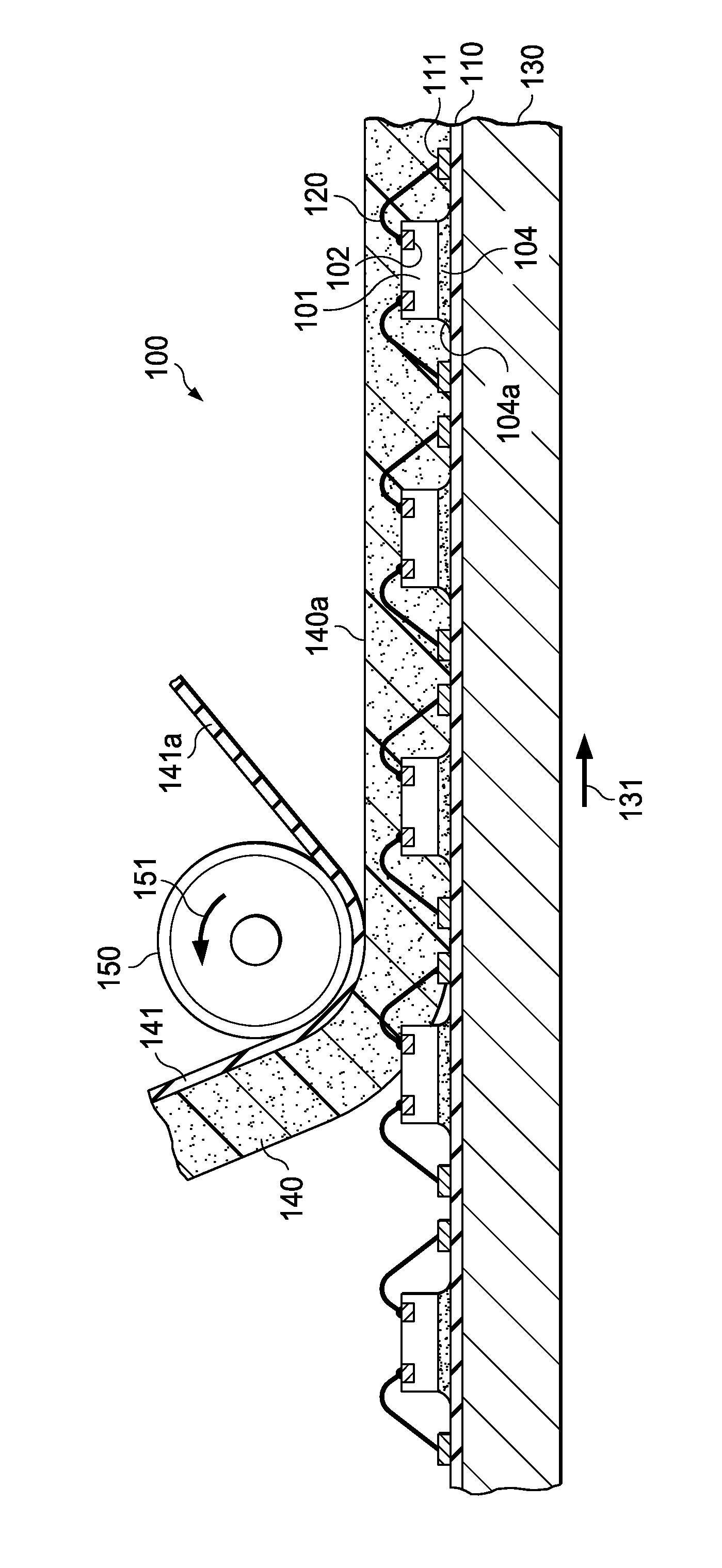
[0017]The schematic FIG. 1 depicts in simplified manner an apparatus, generally designated 100, for executing the encapsulation method of semiconductor devices according to the invention. In FIG. 1, a plurality of semiconductor chips 101 with terminals 102 is assembled on an insulating substrate strip 110. In FIG. 1, substrate 110 is shown as a strip; alternatively, the substrate may be a sheet, on which the chips are arranged in a two-dimensional array. A variety of materials may be used as base material for the substrate. When the overall device thickness has to be kept at a low value, substrate 110 may be a plastic foil made of a polyimide compound in the thickness range from about 40 to 80 μm. Alternatively, substrate may be a somewhat thicker insulating board made of ceramic or FR-4. Integral with substrate 110 are conductive traces and through-holes; substrate 110 further has metallic contact pads 111 on its surface of chip attachment, suitable for metallic wire attachment, an...


PUM


Abstract

A low-viscosity resin is deposited using an apparatus with a movable and heatable wheel and a heater stage. A tape is provided, which includes a layer (140) of an adhesive polymeric resin and a film (141) of an inert plastic compound. The tape is wrapped around the wheel (150) so that the film touches the wheel and the layer faces away from the wheel. The wheel is heated to a temperature high enough to transits the polymeric resin into a low-viscosity state. A substrate strip (110), which has been assembled with a plurality of semiconductor chips (101) connected to the substrate by bonding wires (120), is placed on a station (130) also heated to the transition temperature. The wheel is then moved to roll the low viscosity resin on the chips and wires along the strip, while the inert film is separated. The chips and wires are thus encapsulated.

Description

RELATED APPLICATIONS[0001]This application claims the benefit of provisional application Ser. No. 60 / 977,725 filed Oct. 5, 2007.FIELD OF THE INVENTION[0002]The present invention is related in general to the field of semiconductor devices and processes, and more specifically to the structure and fabrication method of plastic packages for semiconductor devices based on a roll-on encapsulation technique.DESCRIPTION OF RELATED ART[0003]Ever since its introduction in the early 1960's, the transfer molding technology has been the favored method for encapsulating semiconductor devices in plastic packages. In this method, the semiconductor chip is first assembled on a substrate such as a leadframe by physically attaching the chip to the substrate and conductively connecting the chip terminals to the substrate pads, most commonly by arching spans of bonding wire. Then, the substrate together with the assembled chip is transferred to a mold press and positioned in the mold cavity. The cavity ...

Claims


Application Information

Patent Timeline
IPC IPC(8): H01L21/00
CPCH01L21/56H01L24/48H01L23/3121H01L24/97H01L2221/68395H01L2224/48091H01L2224/48465H01L2224/73265H01L2224/97H01L2924/01029H01L2924/01032H01L2924/01047H01L2924/01079H01L2924/01082H01L2924/12044H01L2924/14H01L21/561H01L2224/45144H01L2924/01087H01L2924/01033H01L2924/01019H01L2924/01006H01L2924/01005H01L2924/00014H01L2224/85H01L2224/83H01L2924/00H01L2224/45015H01L2224/45147H01L2924/181H01L24/45H01L2924/20755H01L2924/2075H01L2924/20754H01L2224/05599H01L2924/00012
Inventor ANO, KAZUAKI
Owner TEXAS INSTR INC
Why Eureka
Try Eureka