Solid state imaging device, method of manufacturing the same, and imaging apparatus

a solid-state imaging and manufacturing method technology, applied in the direction of color television, television system, radio control device, etc., can solve the problems of difficult to realize a sufficient hole accumulation layer, the hole accumulation layer does not function as a hole accumulation layer, and the photoelectric conversion characteristic deteriorates, etc., to achieve a small exposure amount, reduce the noise of an imaged image, and improve the effect of image quality

Active Publication Date: 2009-04-16
SONY CORP
View PDF7 Cites 45 Cited by
  • Summary
  • Abstract
  • Description
  • Claims
  • Application Information

AI Technical Summary

Benefits of technology

[0032]In the solid state imaging device according to the embodiment of the present invention, a noise in an imaged image can be reduced because a dark current can be suppressed. As a result, there is an advantage that a high-quality image can be obtained. In particular, generation of a white point (point of a primary color in the case of a color CCD) due to a dark current at the time of long-time exposure with a small exposure amount can be reduced.
[0033]In the method of manufacturing a solid state imaging device according to the embodiment of the present invention, a noise in an imaged image can be reduced because a dark current can be suppressed. As a result, there is an advantage that a solid state imaging device capable of obtaining a high-quality image

Problems solved by technology

In this case, however, diffusion of impurities occurs and a photoelectric conversion characteristic deteriorates.
As a result, the hole accumulation layer does not sufficiently function as a hole accumulation lay

Method used


Image

  • Solid state imaging device, method of manufacturing the same, and imaging apparatus
  • Solid state imaging device, method of manufacturing the same, and imaging apparatus
  • Solid state imaging device, method of manufacturing the same, and imaging apparatus

Examples


Embodiment Construction

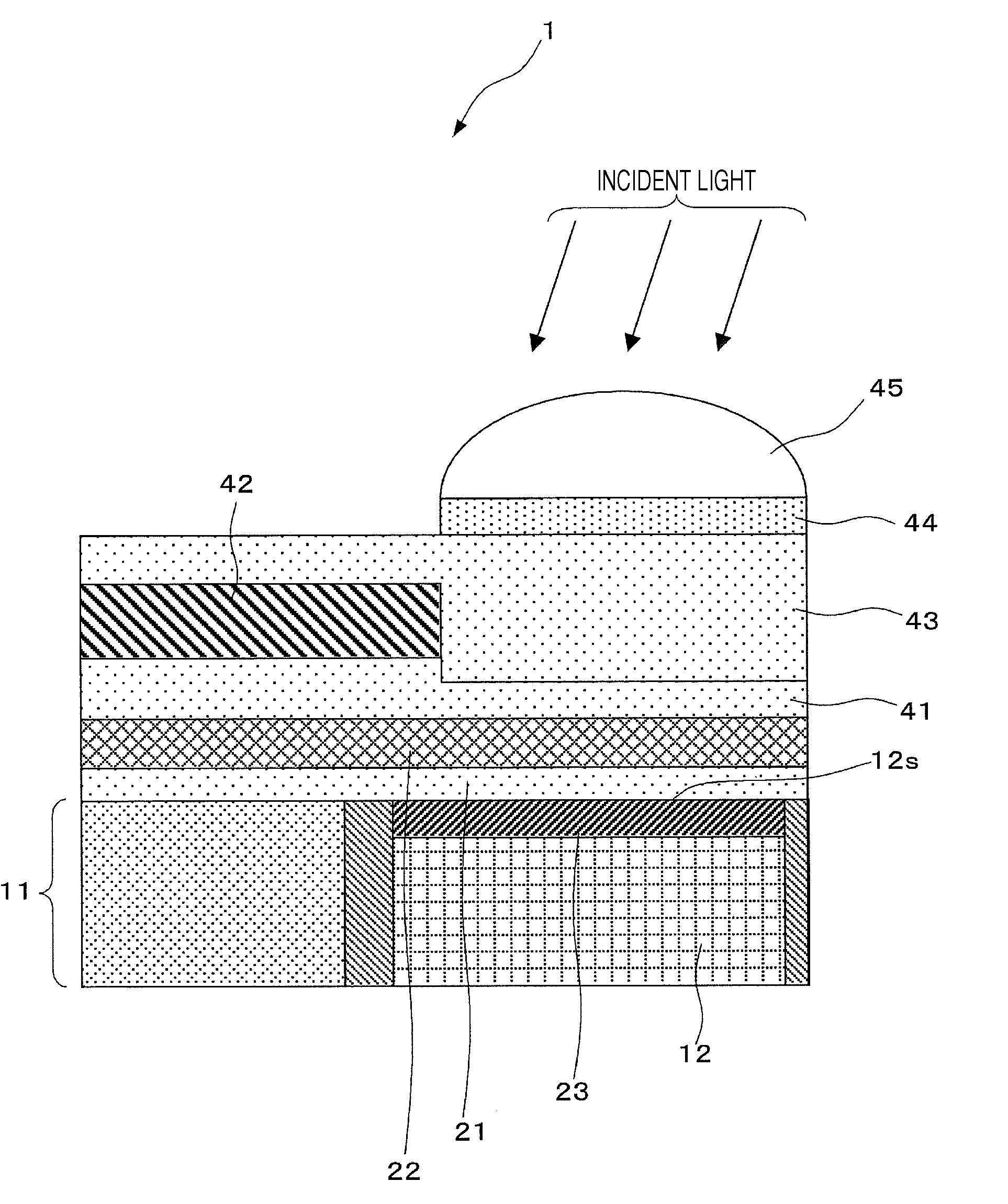
[0077]A solid state imaging device (first solid state imaging device) according to an embodiment (first example) of the present invention will be described with reference to a cross-sectional view of FIG. 1 illustrating the configuration of main parts.

[0078]As shown in FIG. 1, a solid state imaging device 1 includes a light sensing section 12, which performs photoelectric conversion of incident light L, in a semiconductor substrate (or a semiconductor layer) 11. On a side portion of the light sensing section 12, a peripheral circuit section 14 in which a peripheral circuit (not specifically shown) is formed with a pixel separating region 13 interposed therebetween is provided. The following explanation will be made using the semiconductor substrate 11. On a light receiving surface 12s of the light sensing section (including a hole accumulation layer 23 which will be described later) 12, an interface state lowering layer 21 is formed. The interface state lowering layer 21 is formed o...


PUM


Abstract

A solid state imaging device having a light sensing section that performs photoelectric conversion of incident light includes: an insulating layer formed on a light receiving surface of the light sensing section; a layer having negative electric charges formed on the insulating layer; and a hole accumulation layer formed on the light receiving surface of the light sensing section.

Description

CROSS REFERENCES TO RELATED APPLICATIONS[0001]The present invention contains subject matter related to Japanese Patent Application JP 2007-265287 filed in the Japanese Patent Office on Oct. 11, 2007, the entire contents of which being incorporated herein by reference.BACKGROUND OF THE INVENTION[0002]1. Field of the Invention[0003]The present invention relates to a solid state imaging device capable of suppressing generation of a dark current, a method of manufacturing the same, and an imaging apparatus.[0004]2. Description of the Related Art[0005]Solid state imaging devices, such as a CCD (charge coupled device) and a CMOS image sensor, are widely used in a video camera, a digital still camera, and the like. Improvement in sensitivity and noise reduction are important issues in all kinds of solid state imaging devices.[0006]In particular, a dark current, which is detected as a very small current when an electric charge (electron) generated from a minute defect in a substrate interfa...

Claims


Application Information

Patent Timeline
IPC IPC(8): H01L31/0232H01L31/102H01L31/18H01L27/146H01L27/148H01L31/00H01L31/10H04N5/335H04N5/361H04N5/369
CPCH01L27/1461H01L27/1462H01L27/14629H01L27/14643H01L27/14683H01L27/1464H01L27/14621H01L27/14623H01L27/14625H01L27/14627H01L27/14636H01L27/14645H01L27/14818H01L27/14868H01L27/148H01L31/10
Inventor OSHIYAMA, ITARUANDO, TAKASHIHIYAMA, SUSUMUYAMAGUCHI, TETSUJIOHGISHI, YUKOIKEDA, HARUMI
Owner SONY CORP
Why Eureka
Try Eureka