Package substrate and method for fabricating the same
- Summary
- Abstract
- Description
- Claims
- Application Information
AI Technical Summary
Benefits of technology
Problems solved by technology
Method used
Image
Examples
first embodiment
[0041]Please refer to FIGS. 4A through 4G, which are cross-sectional views illustrating the first embodiment of fabrication method of package substrate of the present invention.
[0042]As shown in FIG. 4A, provide a substrate body 40 with a die attaching side 40a and a ball implanting side 40b opposite each other, the die attaching side 40a and the ball implanting side 40b have a plurality of wire bonding pads 401 and a plurality of solder ball pads 402 respectively; form a first insulating passivation layer 41a and a second insulating passivation layer 41b on the die attaching side 40a and the ball implanting side 40b respectively, and then form a plurality of first apertures 410a and a plurality of second apertures 410b in the first insulating passivation layer 41a and the second insulating passivation layer 41b respectively to correspondingly expose the wire bonding pads and the solder ball pads. There are various related techniques for fabricating substrate bodies, the related tec...
second embodiment
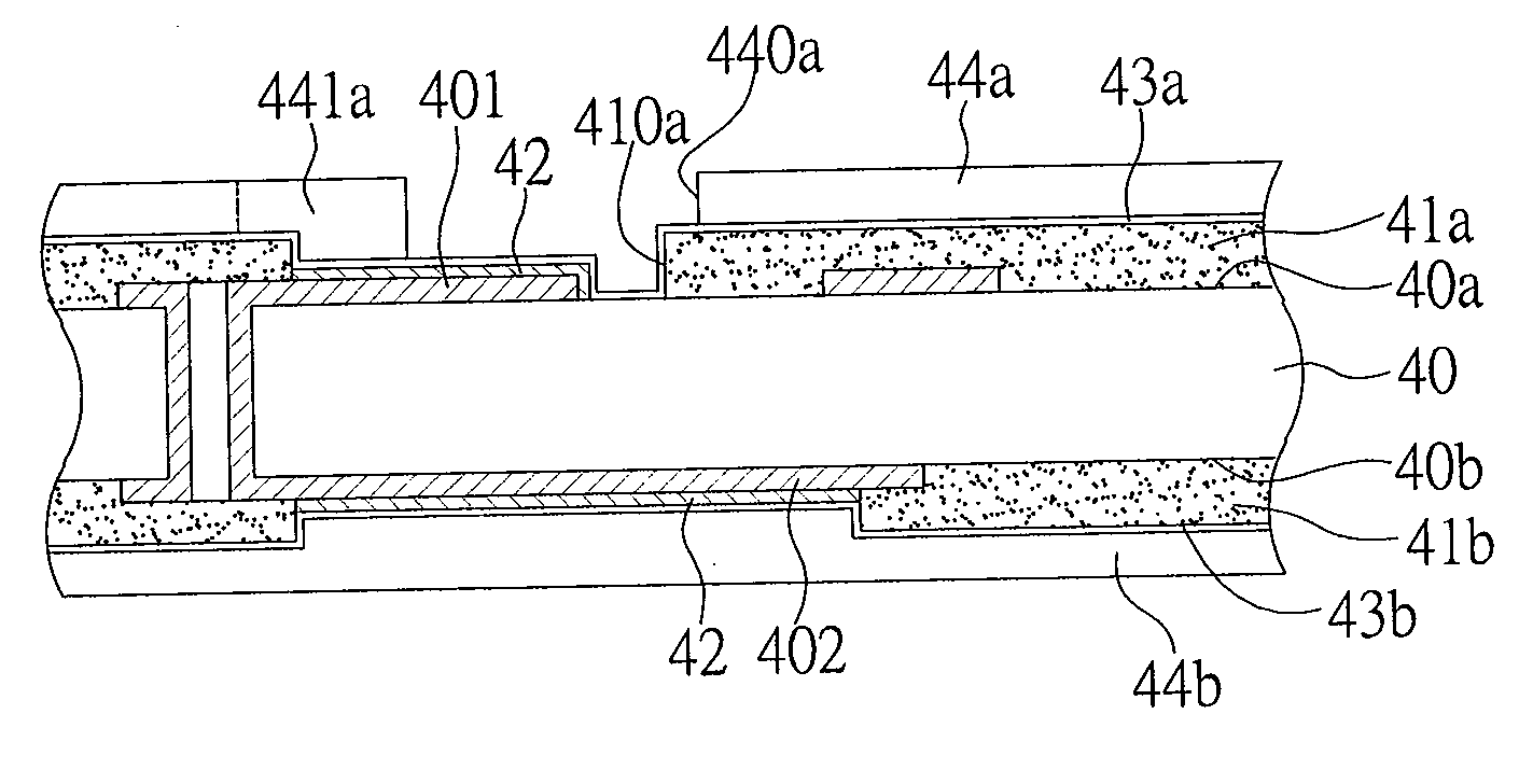
[0048]Please refer to FIGS. 5A through 5E, which are cross-sectional views of the second embodiment of fabrication method of package substrate of the present invention.
[0049]As shown in FIGS. 5A and 5A′, provide first a structure as previously illustrated by FIG. 4C of the first embodiment, and then form a first solder mask 44a on the first conductive layer 43a, and also form a plurality of first openings 440a in the first solder mask 44a to correspondingly expose the first conductive layer 43a on area of the wire bonding pads 401, and the first openings 440a are smaller than the first apertures 410a of the first insulating passivation layer 41a to consequently cover part of the first conductive layer 43a on the wire bonding pads 401; and as shown in FIG. 5A, form a second solder mask 44b on the second conductive layer 43b, or, in accordance with structure illustrated by foregoing FIG. 4C′, as shown in FIG. 5A′, form a second solder mask 44b on the second insulating passivation laye...
third embodiment
[0054]Please refer to FIGS. 6A through 6E, which are cross-sectional views of the third embodiment of fabrication method of package substrate of the present invention, a main difference between both foregoing embodiments is that plating lines 403 collectively function as an electrical conduction path to form a wire bonding metal layer on the wire bonding pads by means of electroplating.
[0055]As shown in FIG. 6A, provide a structure as illustrated in FIG. 4A of the first embodiment, wherein the wire bonding pads 401 are electrically connecting to the plating lines 403.
[0056]As shown in FIG. 6B, form a chemical plating metal layer 42 on the wire bonding pads 401 of the die attaching side 40a and the solder ball pads 402 of the ball implanting side 40b of the substrate body 40 respectively.
[0057]As shown in FIG. 6C, form a second solder mask 44b on the second insulating passivation layer 41b and the chemical plating metal layer 42 of the solder ball pads 402, but the first insulating p...
PUM
 Abstract
Description
Claims
Application Information


