Semiconductor element and method for manufacturing same

a technology of semiconductor elements and semiconductors, applied in the direction of semiconductor devices, basic electric elements, electrical equipment, etc., can solve the problems of reducing the efficiency of the device, affecting the performance of the device, so as to reduce the gate width, the effect of reducing the resistance or on-state current, and minimizing the deterioration of performan

Active Publication Date: 2009-04-23
PANASONIC CORP
View PDF0 Cites 25 Cited by
  • Summary
  • Abstract
  • Description
  • Claims
  • Application Information

AI Technical Summary

Benefits of technology

[0045]In a semiconductor device according to the present invention, including n- and p-type semiconductor regions on the surface of a semiconductor layer and a conductor with a conductive surface that contacts with those semiconductor regions, even if the conductive surface has misaligned with the semiconductor regions, the deterioration in performance due to the misalignment can be minimized. As a result, the present invention always guarantees device performance at an acceptable level.
[0046]Particularly when the present invention is applied to a vertical MOSFET, even if a source electrode being formed on a semiconductor layer by a photolithographic process has misaligned with a contact region that has been defined on the surface of the semiconductor layer, a substantial decrease in gate width can be avoided, and therefore, the decrease in ON-state resistance or ON-state current that could be caused by the misalignment can be minimized. On top of that, the variation in ON-state resistance between products can also be reduced significantly.
[0047]Furthermore, according to the present invention, such a semiconductor device can be fabricated without complicating the manufacturing process.

Problems solved by technology

An electrical circuit with such a coil, however, will produce induced current during switching.
Then, part of the induced current could fail to flow toward the source electrode 109 but a huge amount of current would flow instantaneously around the channel layer 106, thus possibly damaging the channel or gate portion of the MOSFET.

Method used


Image

  • Semiconductor element and method for manufacturing same
  • Semiconductor element and method for manufacturing same
  • Semiconductor element and method for manufacturing same

Examples


embodiment 1

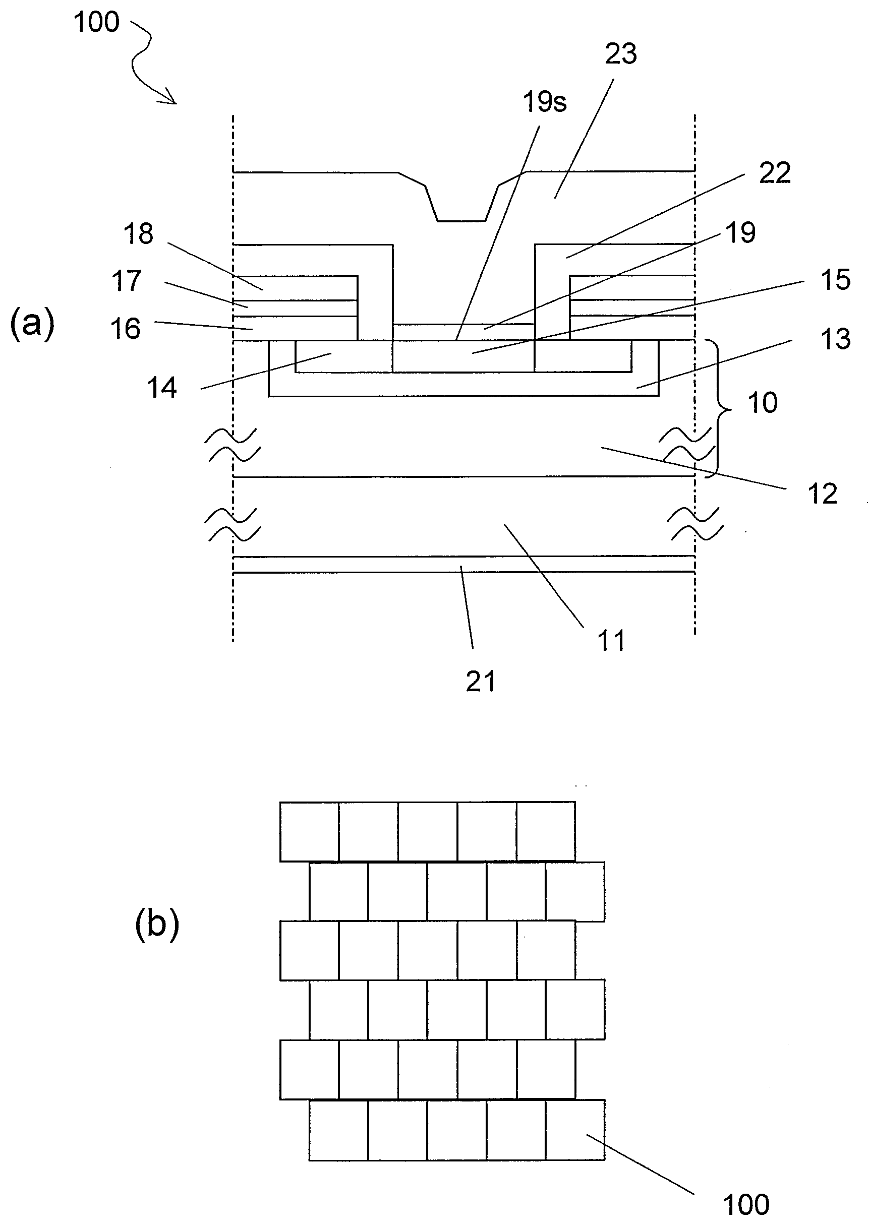
[0094]Hereinafter, a First Specific Preferred Embodiment of a semiconductor device according to the present invention will be described with reference to the accompanying drawings. The semiconductor device of this preferred embodiment is a vertical MOSFET that uses silicon carbide.

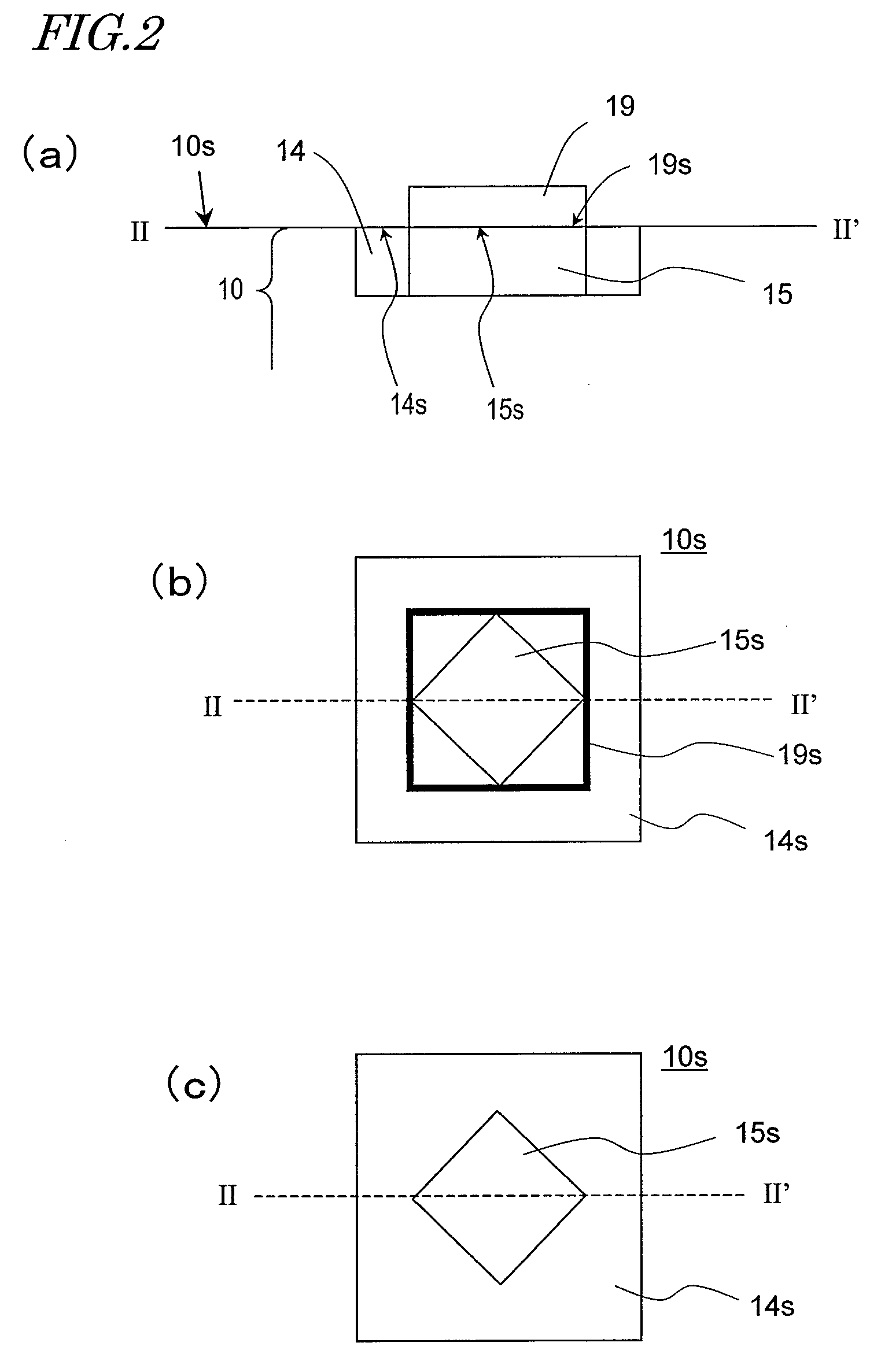
[0095]The semiconductor device of this preferred embodiment includes at least one unit cell including a semiconductor layer, source and drain electrodes that are electrically connected to the semiconductor layer, and a gate electrode for use to switch the semiconductor device between ON and OFF states, and typically has a structure in which a number of such unit cells are arranged. In the following description, a semiconductor device consisting of a plurality of unit cells with a substantially quadrangular planar shape will be taken as an example.

[0096]FIGS. 1(a) and 1(b) are respectively a schematic cross-sectional view illustrating a unit cell of this preferred embodiment and a plan view illustrating an ...

embodiment 2

[0150]Hereinafter, a second preferred embodiment of a semiconductor device according to the present invention will be described with reference to the accompanying drawings. The semiconductor device of this preferred embodiment is a vertical MOSFET that uses silicon carbide but consists of striped unit cells unlike the counterpart shown in FIGS. 1 and 2. In the following description, a comb shaped MOSFET, unit cells of which have stripes that run perpendicularly to the direction in which electrons flow through the channel, will be described as an example.

[0151]FIG. 13(a) is a schematic cross-sectional view illustrating an exemplary unit cell as a second preferred embodiment of the present invention. FIG. 13(b) is a top view illustrating the arrangement of the unit cells in the semiconductor device of this preferred embodiment. For the sake of simplicity, any pair of components shown in both FIGS. 1(a) and 1(b) and FIGS. 13(a) and 13(b) and having substantially the same function is id...


PUM


Abstract

A semiconductor device includes: a semiconductor layer 10; a semiconductor region 15s of a first conductivity type defined on the surface 10s of the semiconductor layer; a semiconductor region 14s of a second conductivity type defined on the surface 10s of the semiconductor layer to surround the semiconductor region 15s; and a conductor 19 with a conductive surface 19s to contact with the semiconductor regions 15s and 14s. The semiconductor layer 10 includes silicon carbide. At least one of the semiconductor region 15s and the conductive surface 19s is not circular. The semiconductor region 15s and the conductive surface 19s are shaped such that as the degree of misalignment between the conductive surface 19s and the semiconductor region 15s increases from zero through one-third of the width of the conductive surface 19s, a portion of the profile of the conductive surface 19s that crosses the semiconductor region 15s has smoothly changing lengths.

Description

TECHNICAL FIELD[0001]The present invention relates to a semiconductor device and a method for fabricating the same.BACKGROUND ART[0002]Silicon carbide (SiC) is a high-hardness semiconductor material with a greater bandgap than silicon (Si), and has been used extensively in various types of semiconductor devices including power elements, hostile-environment elements, high temperature operating elements, and radio frequency elements. Among other things, the application of SiC to power elements such as switching elements and rectifiers has attracted a lot of attention. This is because a power element that uses SiC can significantly reduce the power loss compared to a Si power element.[0003]Among various power elements that use SiC, switching elements such as a MOSFET and a MESFET are known as typical ones. Such a switching element can switch between ON state in which drain current of several amperes (A) or more flows and OFF state in which the drain current becomes zero by changing the...

Claims


Application Information

Patent Timeline
Patent Type & Authority Applications(United States)
IPC IPC(8): H01L29/12H01L21/04
CPCH01L21/046H01L29/0696H01L29/1608H01L29/7828H01L29/66068H01L29/7802H01L29/41741
Inventor UCHIDA, MASAOHASHIMOTO, KOICHIHAYASHI, MASASHI
Owner PANASONIC CORP
Why Eureka
Try Eureka