Pellicle and method for manufacturing the same

a technology of pellicle and euv, which is applied in the field of pellicle for lithography, can solve the problems of many technical problems that must be solved in order to realize a pellicle for euv, many unsolved problems, and achieve the effect of superior transmittance and chemical stability

Active Publication Date: 2009-04-23
SHIN ETSU CHEM IND CO LTD
View PDF7 Cites 23 Cited by
  • Summary
  • Abstract
  • Description
  • Claims
  • Application Information

AI Technical Summary

Benefits of technology

[0021]In the present invention, a silicon crystal film, the absorption coefficient of which is 0.005/nm or lower with respect to light having a wavelength of 13.5 nm, is u

Problems solved by technology

With lithography based on such excimer exposure techniques as described above, however, it is considered difficult to cope with patterning requiring further miniaturization in which a pattern width is 32 nm or less.
On the other hand, many technical problems that must be solved in order to realize a pellicle for EUV remain unsolved in the development of the pellicle.
The present situation is, however, that no solutions have yet been in sight to the problem of developing practical pellicle film materials superior in transmittance and chemical stability.
However, the silicon used as a

Method used


Image

  • Pellicle and method for manufacturing the same
  • Pellicle and method for manufacturing the same
  • Pellicle and method for manufacturing the same

Examples


embodiment 1

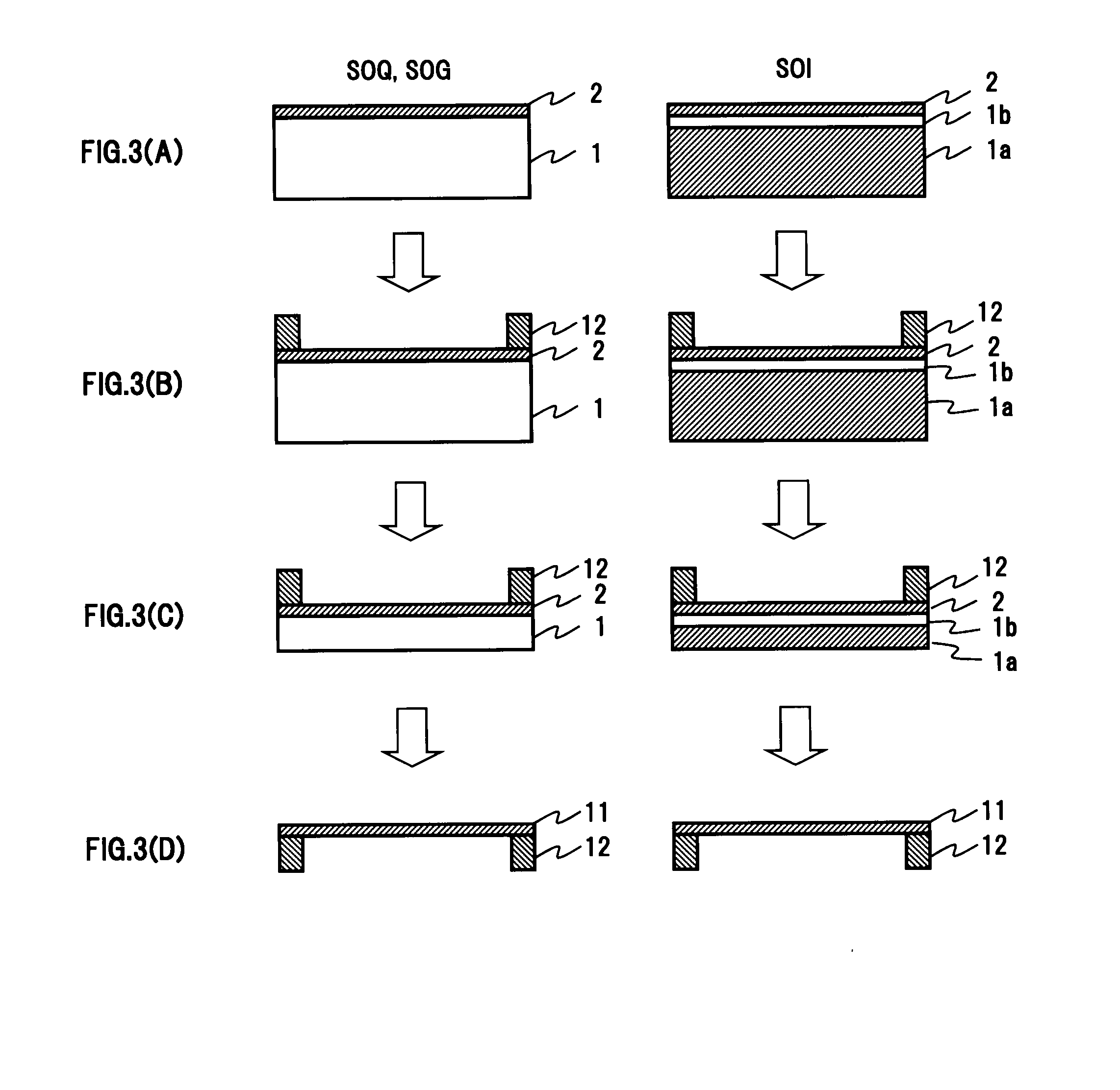
[0039]FIGS. 3(A) to 3(D) are schematic views used to explain process examples of a method for manufacturing a pellicle of the present invention. The supporting substrate 1 of an SOI (Silicon On Insulator) substrate illustrated in FIG. 3(A) is a substrate in which an oxide film 1b is provided on a surface of a silicon substrate 1a. The supporting substrates 1 of an SOQ (Silicon On Quartz) substrate and an SOG (Silicon On Glass) substrate are a quartz substrate and a glass substrate, respectively. On a principal surface of each of these supporting substrates 1, there is provided a single-crystal silicon crystal film 2 and this silicon crystal film 2 becomes a pellicle film.

[0040]The silicon substrate 1a serving as the supporting substrate of the SOI substrate is a commercially-available single-crystal silicon substrate grown using, for example, a Czochralski (CZ) method. The oxide film 1b is previously formed on a surface of this single-crystal silicon substrate 1a by means of thermal...

embodiment 2

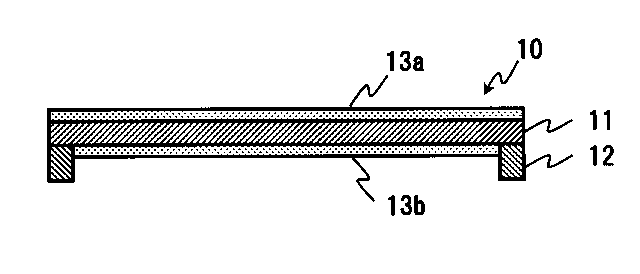
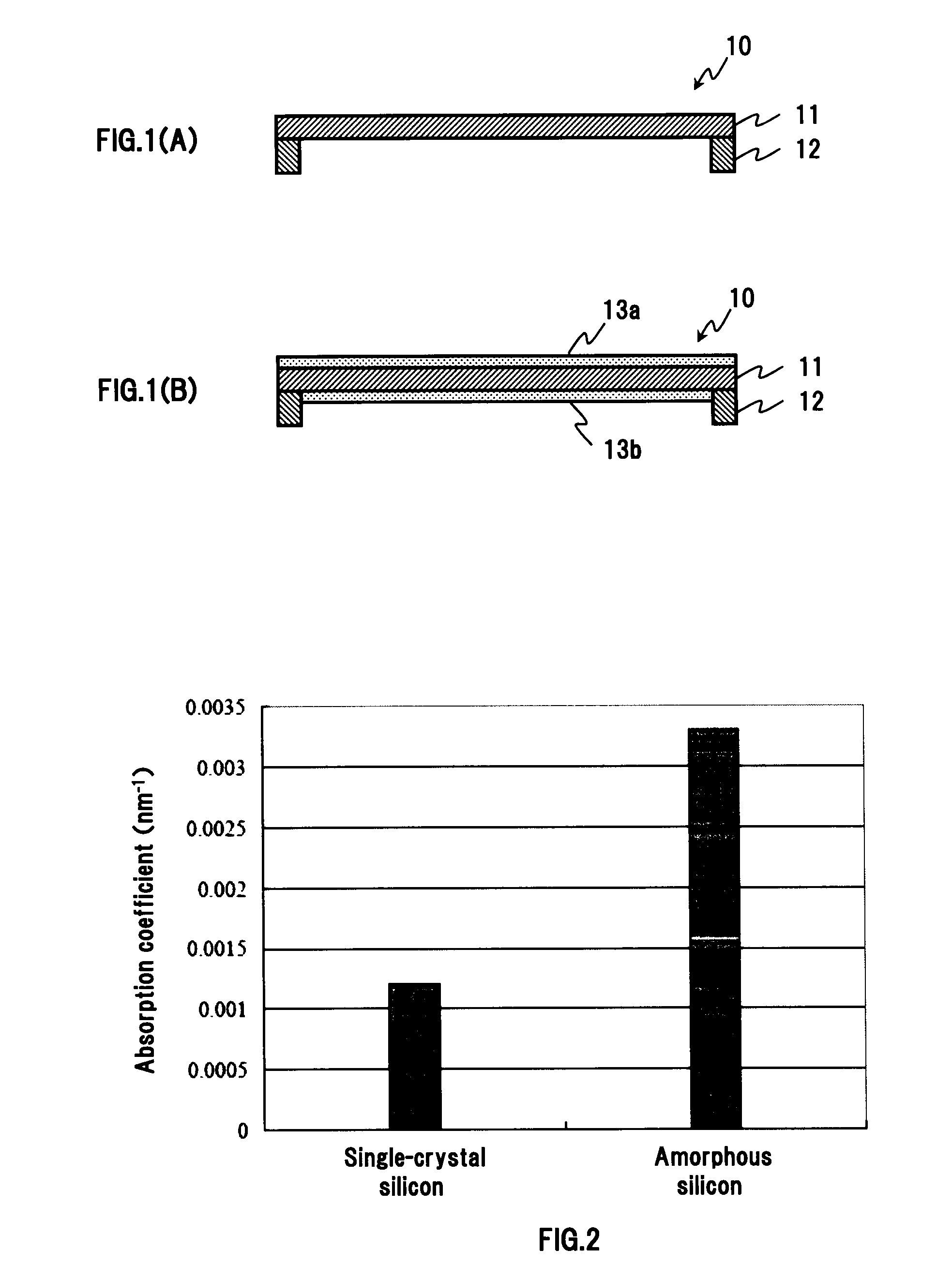
[0048]A silicon crystal film 11 supported by a pellicle frame 12 is obtained according to steps explained using FIGS. 3(A) to 3(D). Note that the thickness of the silicon crystal film 11 of the present embodiment is 20 nm. In addition, a several nanometers thick SiC thin film is deposited respectively on the front and rear surfaces of this silicon crystal film 11 using a gas cluster ion beam deposition method, in order to coat the silicon crystal film.

[0049]It has been confirmed that both of the pellicles obtained in embodiments 1 and 2 have a transmissivity of 50% or higher with respect to EUV light, show a practical-use level of throughput at the time of EUV exposure, and are completely free from degradation in the yield of devices due to foreign matter.

[0050]As described heretofore, the present invention provides a pellicle provided with a practical pellicle film for EUV superior in transmittance and chemical stability.


PUM


Abstract

A pellicle of the present invention is provided with a silicon crystal film, the absorption coefficient of which is 0.005/nm or lower with respect to light having a wavelength of 13.5 nm, as a pellicle film. The silicon crystal film is an indirect transition type semiconductor film and, therefore, the optical absorption coefficient thereof is relatively low. In particular, a single-crystal silicon film has a lower absorption coefficient than an amorphous silicon film and a polysilicon film. Thus, it is easy to obtain desired transmissivity required of a pellicle film for EUV from the single-crystal silicon film. Such a pellicle film as described above can be fabricated from an SOI film obtained by thin-filming an SOI substrate (including an SOQ substrate and an SOG substrate).

Description

BACKGROUND OF THE INVENTION[0001]1. Field of the Invention[0002]The present invention relates to a pellicle for lithography and, more particularly, to a pellicle suitable for lithography using extreme ultraviolet light (EUV: Extreme Ultra-Violet) and a method for manufacturing the pellicle.[0003]2. Description of the Related Art[0004]Along with the increasingly higher integration of a semiconductor device, a pattern to be formed by lithography has been miniaturized. Nowadays, even a device having a pattern width of 45 nm or so is being put into practical use. Such a thin-line pattern can be realized by lithography using an ArF immersion method, a double exposure method or the like which are improved versions of a conventional excimer exposure technique.[0005]With lithography based on such excimer exposure techniques as described above, however, it is considered difficult to cope with patterning requiring further miniaturization in which a pattern width is 32 nm or less. Hence, litho...

Claims


Application Information

Patent Timeline
IPC IPC(8): G03F1/00G03F1/24G03F1/62
CPCB82Y10/00G03F1/62G03F1/24B82Y40/00
Inventor KUBOTA, YOSHIHIROAKIYAMA, SHOJISHINDOO, TOSHIHIKO
Owner SHIN ETSU CHEM IND CO LTD
Why Eureka
Try Eureka