

Thermal Gradient Control of High Aspect Ratio Etching and Deposition Processes
a technology of etching and deposition process, applied in the direction of coatings, semiconductor devices, decorative arts, etc., can solve the problems of limiting the aspect ratio of deposited materials, pinching, and various physical limitations of circuit elements and their interconnection structures, and achieve the effect of reducing or eliminating the pinching problem
- Summary
- Abstract
- Description
- Claims
- Application Information
AI Technical Summary
Benefits of technology
Problems solved by technology
Method used
Image

Examples
Embodiment Construction
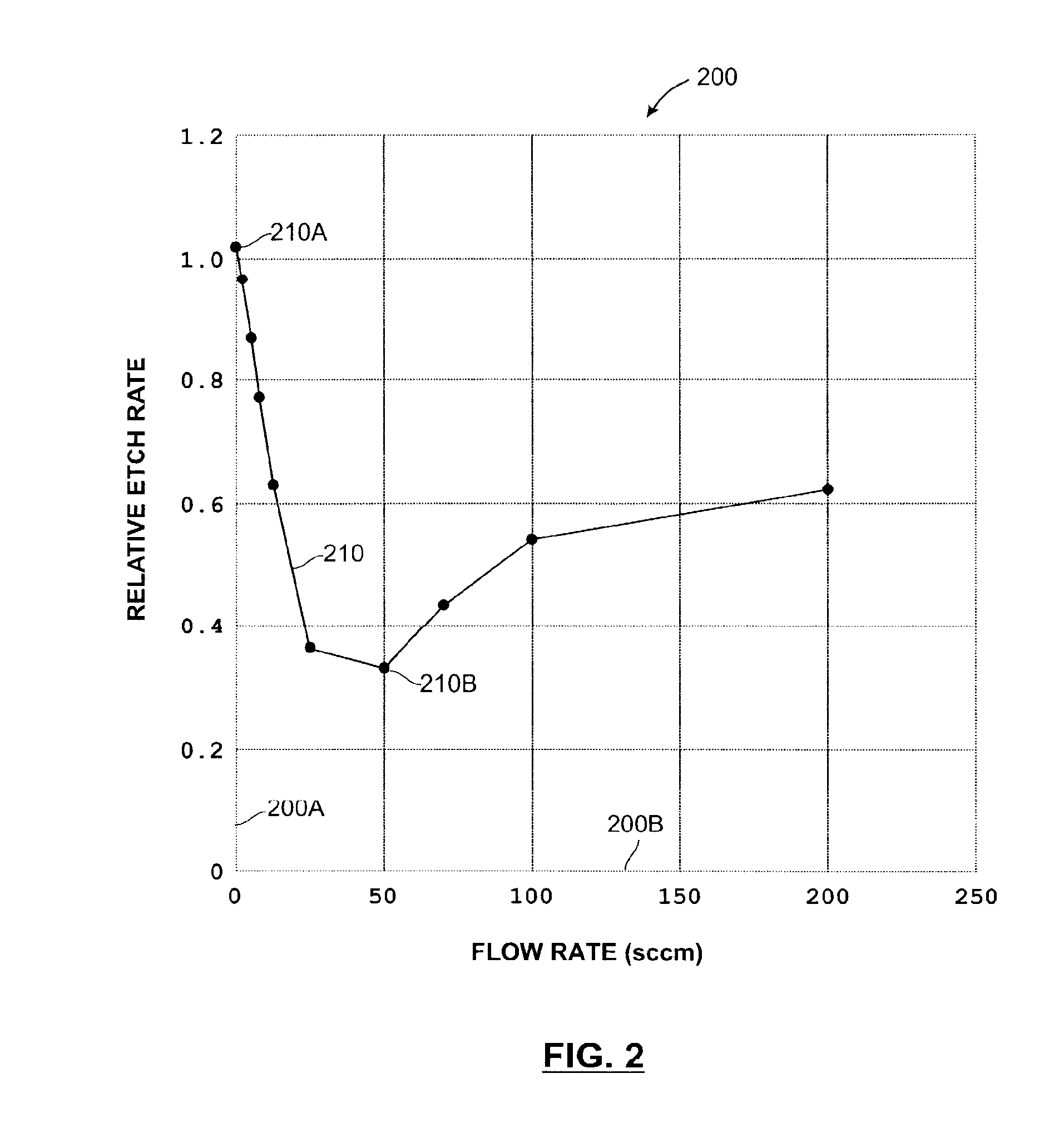
[0027]The present inventive technique makes use of the fact that the rates of certain etching and deposition processes are significantly affected by temperature. By creating temperature differentials in a semiconductor wafer, (e.g., at different depths in a trench) etching and / or deposition can be caused to occur at different rates simultaneously at different locations on the wafer.
[0028]By controlling temperature such that an etch rate is higher at the bottom of a trench than at the top, the rate at which solid reaction products (the aforementioned “crust”) form along the upper sidewalls of the trench can be reduced, thereby eliminating or at least delaying pinch off.
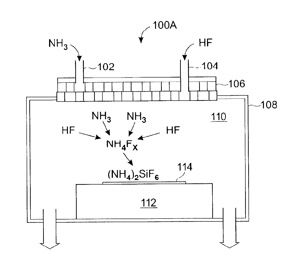
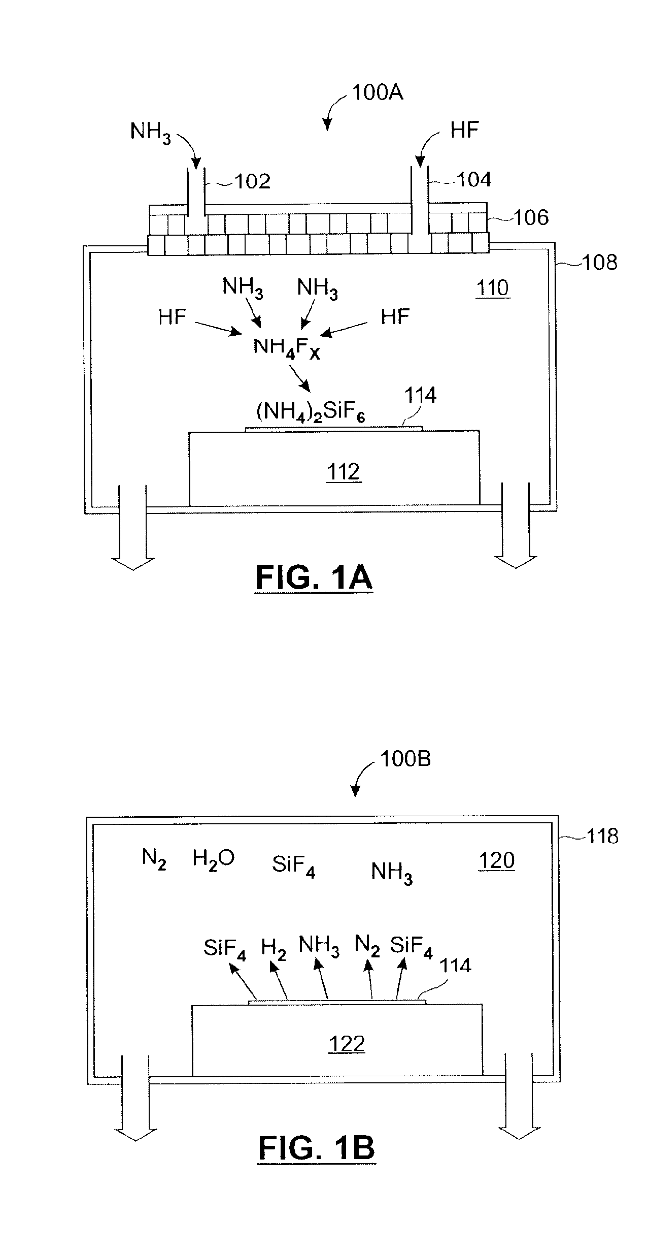
[0029]By way of example, a two-step Chemical Oxide Removal process is shown to be temperature-sensitive. The first step is characterized a reaction between a mixture of gaseous hydrofluoric acid and gaseous ammonia with oxide (silicon dioxide—SiO2) on the surface of a wafer, leaving behind a solid reaction product on t...
PUM
| Property | Measurement | Unit |
|---|---|---|
| temperature | aaaaa | aaaaa |
| temperature | aaaaa | aaaaa |
| reaction rate | aaaaa | aaaaa |
Abstract
Description
Claims
Application Information