Nanoprobe tip for advanced scanning probe microscopy comprising a layered probe material patterned by lithography and/or fib techniques

a scanning probe and advanced technology, applied in the direction of mechanical measurement arrangement, mechanical roughness/irregularity measurement, instruments, etc., can solve the problem of not being able to efficiently extract detailed information on the surface, the more challenging requirements of such a nano-probe have to be taken into account, and the performance degradation of another type of transistor. achieve the effect of high degree of uniformity, enhanced flexibility in shaping the tip portion, and high degree of flexibility

Inactive Publication Date: 2009-05-07
ADVANCED MICRO DEVICES INC
View PDF8 Cites 21 Cited by
  • Summary
  • Abstract
  • Description
  • Claims
  • Application Information

AI Technical Summary

Benefits of technology

[0014]Generally, the subject matter disclosed herein relates to enhanced techniques for the fabrication of nano-probes to obtain respective devices for sophisticated analytical scanning probe microscopy techniques, wherein the probes may be formed with a high degree of uniformity and with a high degree of flexibility with respect to the shaping of the probes. Furthermore, the techniques disclosed herein enable the selection of a wide class of materials for the tip portions of the nano-probes, which, in turn, provides the possibility of adjusting the characteristics of the probe under consideration with respect to the analytical task to be fulfilled, wherein, in combination with enhanced flexibility in shaping the tip portions and in view of the highly uniform process technique, a plurality of scanning probe measurement strategies may be employed as standard metrology strategies during the complex manufacturing process for forming microstructure devices. For this purpose, a probe material may be provided in the form of a layer material on an appropriate carrier material and may be subsequently patterned, which, in some illustrative aspects disclosed herein, may be accomplished on the basis of lithography and / or highly directional particle bombardment, such as a focused ion beam, to obtain the desired shaping of the tip and a cantilever portion connected thereto. Furthermore, the portions of carrier material may be appropriately removed to “expose” or release the cantilever portion and the tip portion. Thus, a wide variety of materials, such as metals, highly doped semiconductor materials, dielectric materials and the like, may be used for the tip portion and the cantilever connected thereto, while the remaining substrate material may be efficiently used as a mechanical support and thus as a remaining cantilever, the deflection of which may be detected on the basis of optical techniques, wherein the required optical characteristics of the substrate material, such as reflectivity and the like, may be efficiently adjusted. Furthermore, for electrically conductive materials, an appropriate interconnection structure may be formed during the patterning of the tip portion and the cantilever portion, thereby further enhancing the flexibility and reliability of the manufacturing technique and thus of the resulting nano-probes. In some illustrative aspects disclosed herein, the carrier material may be pre-processed to obtain a “template” structure prior to providing the probe material, wherein the template structure may act as a “mold” for the probe material, at least in the tip portion, thereby efficiently defining the basic configuration of the tip portion so that, for instance, the degree of tapering of the tip portion, an inclination angle of the probe material with respect to the cantilever portion, and the like may be defined with high uniformity for a plurality of probes on the basis of well-established three-dimensional microstructuring technologies, as may be used for conventional MEMS (microelectronic mechanical structures) or conventional mechanical nano-probes.

Problems solved by technology

When imaging a sample surface with high spatial resolution, respective surface portions within an area of a few micrometers or smaller may appear almost atomically flat so that the corresponding image obtained by means of the scanning probe microscope may include less contrast and thus may not allow efficient extraction of detailed information on surface characteristics at this high resolution, although on a broader scale a significant sample topography may be present.
The strain in the channel regions and / or other transistor areas may have to be specifically applied for the different transistor types, such as N-channel transistors and P-channel transistors, since the type of strain that enhances performance of one type of transistor may result in performance degradation in another type of transistor.
In other aspects involving thermal characteristics of the surface under consideration, as previously mentioned, even more challenging requirements of such a nano-probe have to be taken into consideration.
Thus, a plurality of promising analytical techniques are available on the basis of scanning probe microscopy techniques, which may be used for estimating materials and manufacturing techniques applied for the manufacturing of microstructural devices, such as advanced integrated circuits, wherein, however, the fabrication of appropriate nano-probes on the basis of conventional strategies may reduce the overall efficiency of these promising analytical tools.

Method used


Image

  • Nanoprobe tip for advanced scanning probe microscopy comprising a layered probe material patterned by lithography and/or fib techniques
  • Nanoprobe tip for advanced scanning probe microscopy comprising a layered probe material patterned by lithography and/or fib techniques
  • Nanoprobe tip for advanced scanning probe microscopy comprising a layered probe material patterned by lithography and/or fib techniques

Examples


Embodiment Construction

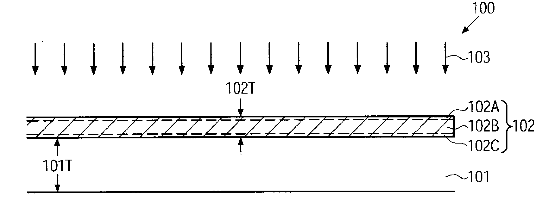
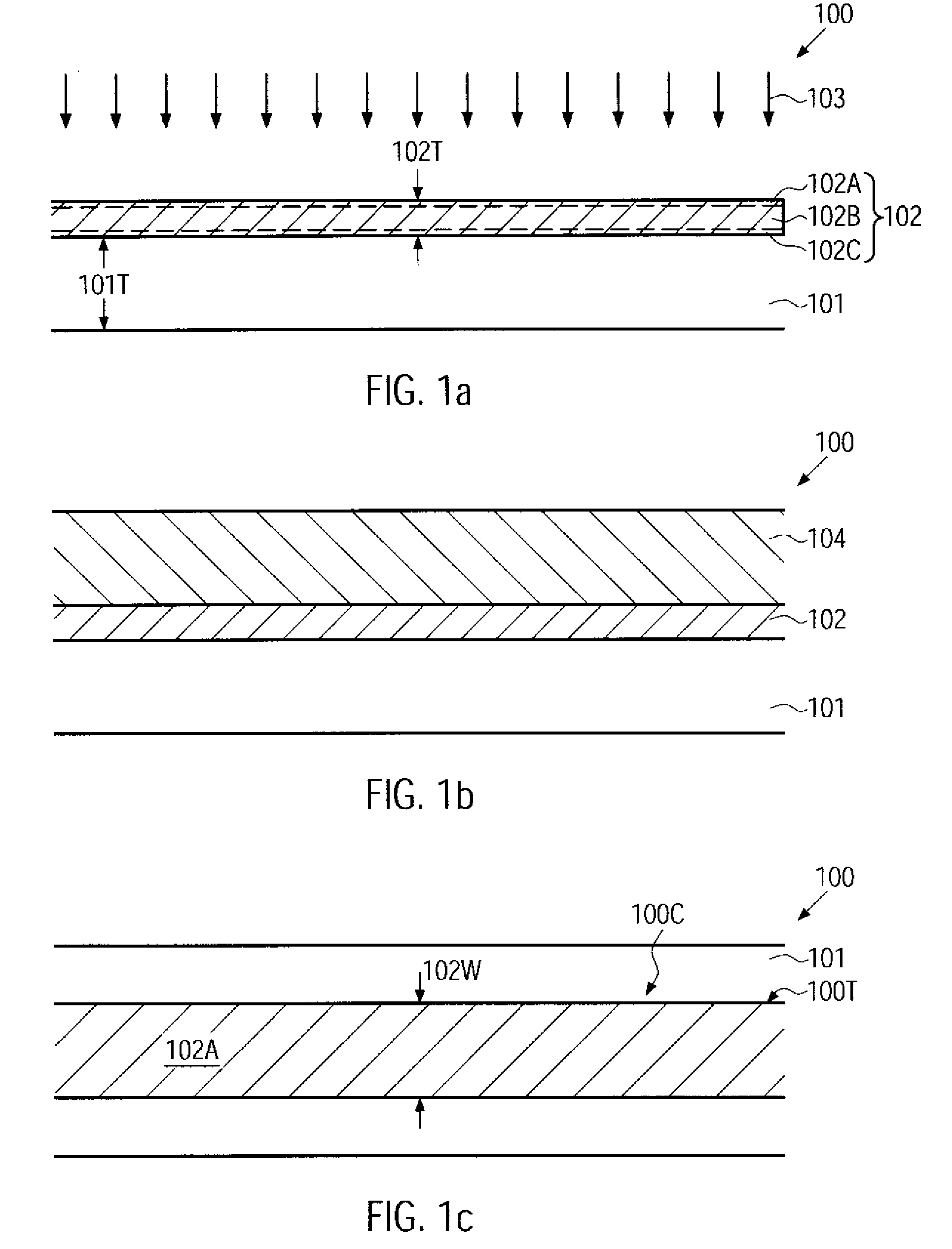
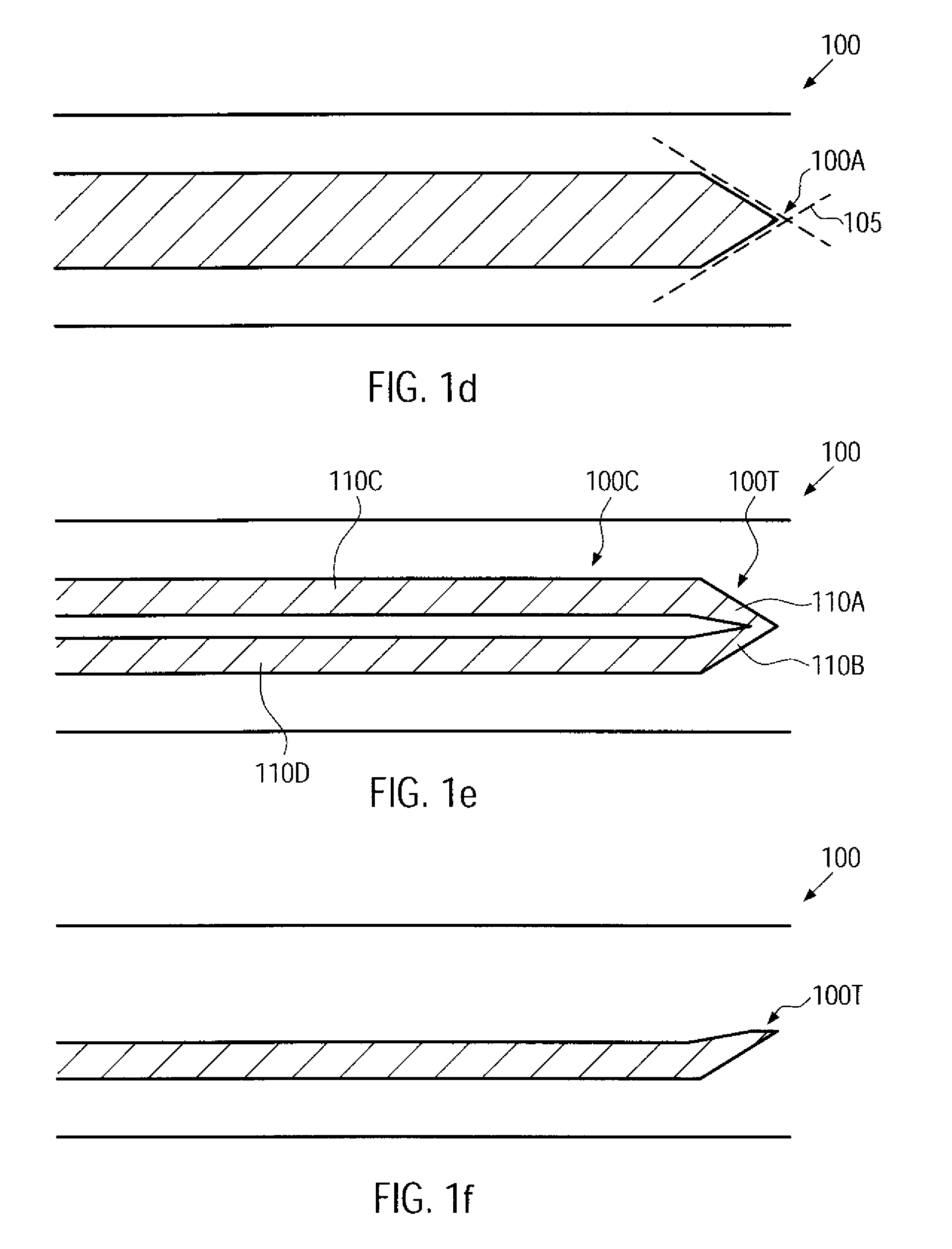
[0033]Various illustrative embodiments of the invention are described below. In the interest of clarity, not all features of an actual implementation are described in this specification. It will of course be appreciated that in the development of any such actual embodiment, numerous implementation-specific decisions must be made to achieve the developers' specific goals, such as compliance with system-related and business-related constraints, which will vary from one implementation to another. Moreover, it will be appreciated that such a development effort might be complex and time-consuming, but would nevertheless be a routine undertaking for those of ordinary skill in the art having the benefit of this disclosure.

[0034]The present subject matter will now be described with reference to the attached figures. Various structures, systems and devices are schematically depicted in the drawings for purposes of explanation only and so as to not obscure the present disclosure with details ...


PUM

PropertyMeasurementUnit
thicknessaaaaaaaaaa
thicknessaaaaaaaaaa
widthaaaaaaaaaa

Abstract

By forming an appropriate material layer, such as a metal-containing material, on a appropriate substrate and patterning the material layer to obtain a cantilever portion and a tip portion, a specifically designed nano-probe may be provided. In some illustrative aspects, additionally, a three-dimensional template structure may be provided prior to the deposition of the probe material, thereby enabling the definition of sophisticated tip portions on the basis of lithography, wherein, alternatively or additionally, other material removal processes with high spatial resolution, such as FIB techniques, may be used for defining nano-probes, which may be used for electric interaction, highly resolved temperature measurements and the like. Thus, sophisticated measurement techniques may be established for advanced thermal scanning, strain measurement techniques and the like, in which a thermal and/or electrical interaction with the surface under consideration is required. These techniques may be advantageously used for failure localization and local analysis during the fabrication of advanced integrated circuits.

Description

BACKGROUND OF THE INVENTION[0001]1. Field of the Invention[0002]Generally, the present disclosure relates to metrology in the manufacturing of micro-structures, such as integrated circuits, and, more particularly, to the measurement of the surface characteristics of microstructure features by means of scanning probe microscopy (SPM) for determining surface and near-surface characteristics with nanometer resolution.[0003]2. Description of the Related Art[0004]In manufacturing microstructures, such as integrated circuits, micromechanical devices, opto-electronic components and the like, device features, such as circuit elements, are typically formed on an appropriate substrate by patterning the surface portions of one or more material layers previously formed on the substrate. Since the dimensions, i.e., the length, width and height, of individual features are steadily decreasing to enhance performance and improve cost-effectiveness, these dimensions have to be maintained within tight...

Claims


Application Information

Patent Timeline
Patent Type & Authority Applications(United States)
IPC IPC(8): G01B5/28B05D5/12C23C14/00G03F7/20G01Q70/12G01Q70/14
CPCG01Q70/14B82Y35/00
Inventor HECKER, MICHAELZSCHECH, EHRENFRIEDGRABIEC, PIOTRJANUS, PAWELGOTSZALK, TEODOR
Owner ADVANCED MICRO DEVICES INC
Why Eureka
Try Eureka