Formation of photoconductive and photovoltaic films

a technology of photovoltaic films and photoconductive materials, which is applied in the direction of vacuum evaporation coating, transportation and packaging, coatings, etc., can solve the problems of low device yield, the deposited lead salt material may not adhere to the substrate properly, and the deposition method has several problems, so as to achieve enhanced chemical vapor deposition

Inactive Publication Date: 2009-05-14
ADVANCED INTEGRATION
View PDF2 Cites 24 Cited by
  • Summary
  • Abstract
  • Description
  • Claims
  • Application Information

AI Technical Summary

Benefits of technology

[0016]The deposition system can include an iodine gas source coupled to the second gas line. The iodine gas source can include a container with solid iodine positioned in it. A heater is positioned to heat the solid iodine forming an iodine gas. A temperature control system is coupled to the container to monitor the temperature of the iodine gas. A pressure control system is also coupled to the container to monitor a pressure of the iodine gas inside the container. A container gas outlet is positioned to allow an amount of the iodine gas in the container to flow to the second gas line. The temperature control system adjusts the amount of heat provided by the heater in response to a feedback signal provided by the pressure control system. The feedback signal indicates the pressure of the iodine gas in the container. In this way, the temperature and pressure of the iodine gas can be controlled so that the amount of iodine gas is flowed through the second gas line.
[0017]The present application further provides a deposition system with a substrate transfer housing having a plurality of openings. A door is coupled to each opening of the substrate transfer housing. Each door is movable between a first position away from the substrate transfer housing and a second position enclosing the substrate transfer housing. A substrate holder chamber is coupled to at least one opening of the substrate transfer housing. At least one sputter deposition system and at least one plasma enhanced chemical vapor deposition (PECVD) system are also coupled to at least one opening of the substrate transfer housing. In this way, a substrate can be transferred between the at least one sputter deposition system and the at least one PECVD system without undesirably exposing the substrate to the outside atmosphere between depositions.

Problems solved by technology

However, these deposition methods have several problems.
One problem is that the deposited lead salt material may not adhere to the substrate properly.
This is particularly a problem if the substrate is silicon.
If the lead salt material does not adhere properly, then the yield of devices is low, which increases the costs.
Another problem is that it is difficult to control the composition of the deposited lead salt material.
This is further complicated because the composition can undesirably change with time after it is deposited and exposed to the outside atmosphere.
A further problem is that it is typically desired to sensitize the lead salt material.
However, the sensitization of lead salt material regions using conventional methods often leads to undesirable differences in resistivity from one lead salt material region to another.
These problems limit the usefulness of any devices formed with lead salt materials fabricated using conventional deposition systems and methods.

Method used


Image

  • Formation of photoconductive and photovoltaic films
  • Formation of photoconductive and photovoltaic films
  • Formation of photoconductive and photovoltaic films

Examples


Embodiment Construction

[0033]While exemplary embodiments are described herein in sufficient detail to enable those skilled in the art to practice the invention, it should be understood that other embodiments may be realized and that logical electrical and mechanical changes may be made without departing from the spirit and scope of the invention. Thus, the following detailed description is presented for purposes of illustration only.

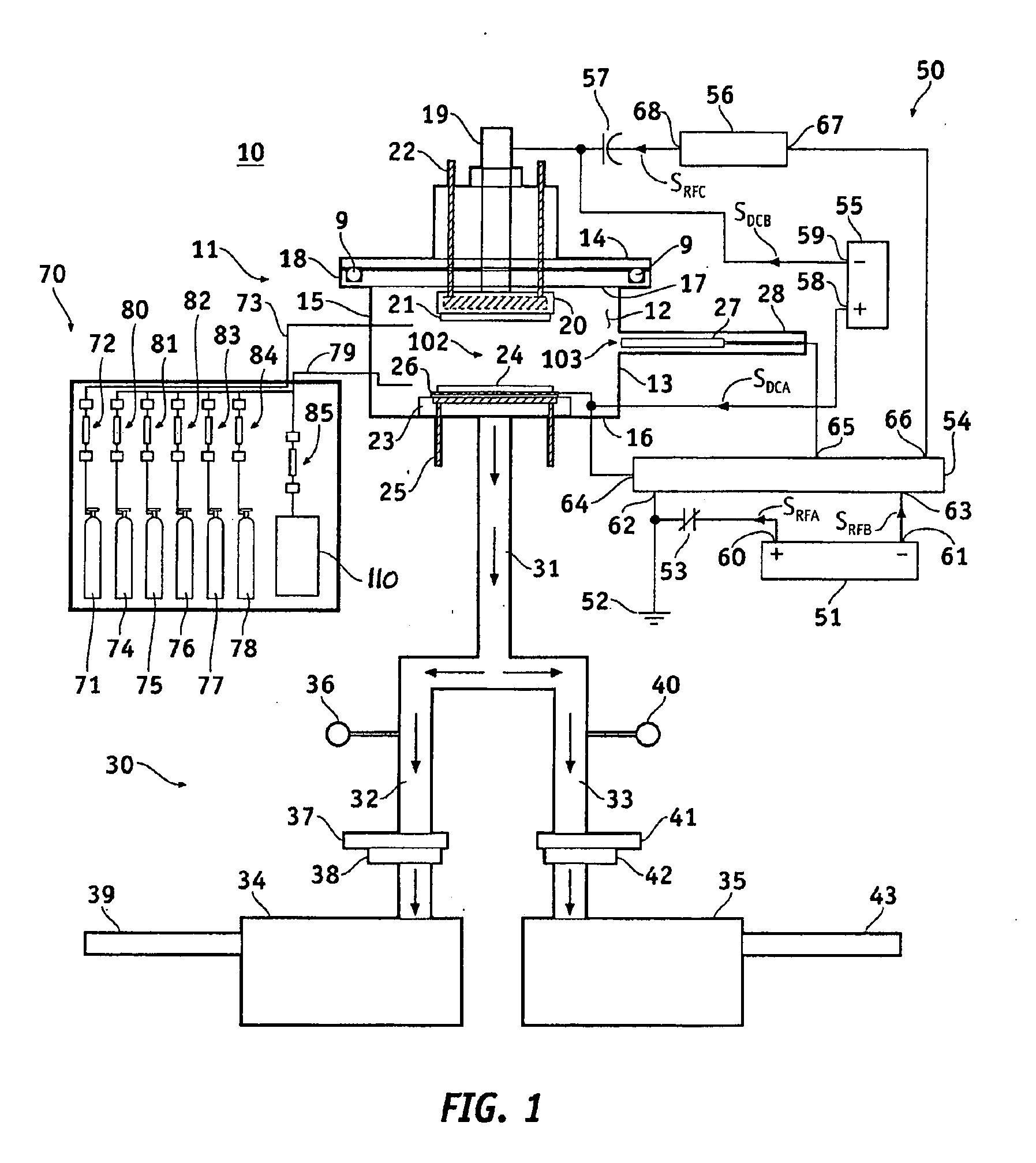
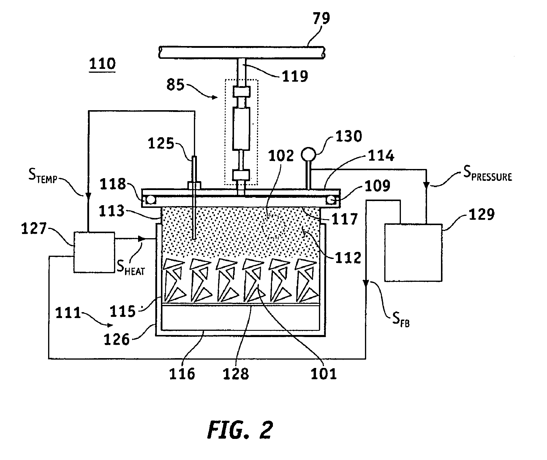
[0034]Turning now to the drawings, in which like reference characters indicate corresponding elements throughout the several views, attention is first directed to FIG. 1 which shows a simplified diagram of a deposition system 10 in accordance with the present invention. Deposition system 10 allows the deposition of separate material regions onto a substrate by sputtering and plasma enhanced chemical vapor deposition (PECVD) without undesirably exposing them to the outside atmosphere in between depositions.

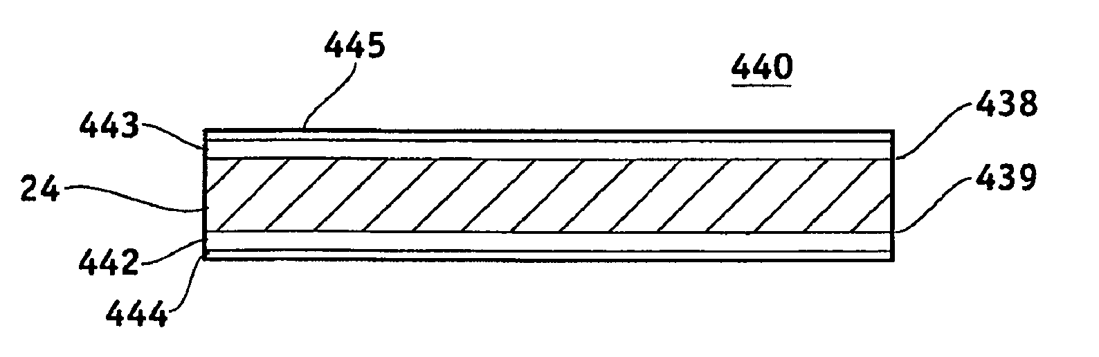
[0035]Some of the material regions can include lead salt materials such ...


PUM

PropertyMeasurementUnit
atmospheric pressureaaaaaaaaaa
pressureaaaaaaaaaa
temperatureaaaaaaaaaa

Abstract

The present application discloses a method and system of depositing a lead selenide film onto another material. The lead selenide film may used in a photoconductive application or a photovoltaic application. Furthermore, the applications may be responsive to infrared radiation at ambient temperature. In one embodiment, a method includes sputtering the lead selenide film, performing a sensitization process, and applying a passivation film. In one exemplary embodiment, a p-n junction is formed by directly adhering a lead selenide film to a silicon substrate.

Description

RELATED APPLICATION[0001]This application is a continuation-in-part of U.S. patent application Ser. No. 11 / 059,981, filed Feb. 17, 2005. The '981 application claims priority to U.S. Provisional Application No. 60 / 545,249, filed Feb. 17, 2004, which is hereby incorporated by reference. Furthermore, this application claims priority to U.S. Provisional Application No. 60 / 985,876, filed Nov. 6, 2007 and to U.S. Provisional Application No. 61 / 025,141, filed Jan. 31, 2008.FIELD OF INVENTION[0002]The present application relates to systems and methods for depositing material regions onto substrates. More specifically, the present application relates to systems and methods for depositing a lead selenide film onto various materials, such as a silicon substrate.BACKGROUND OF THE INVENTION[0003]The use of lead salt materials, such as lead sulfide (PbS), lead selenide (PbSe), and lead telluride (PbTe), in photoconductive and photovoltaic applications is well known in the art. Lead salt materials...

Claims


Application Information

Patent Timeline
Patent Type & Authority Applications(United States)
IPC IPC(8): H01L31/04H01L21/20C23C14/34
CPCC23C14/0623C23C14/34C23C14/3464C23C16/02Y10T428/24942C23C16/50H01J37/32009H01J37/34C23C16/4485
Inventor ENGLE, GEORGE
Owner ADVANCED INTEGRATION
Why Eureka
Try Eureka