Organic light emitting device

a light-emitting device and organic technology, applied in the direction of organic semiconductor devices, discharge tubes/lamp details, discharge tubes luminescent screens, etc., can solve the problem that the voltage typically must be increased to achieve a given luminance, and achieve the effect of reducing power consumption, improving driving voltage characteristics, and reducing voltag

Active Publication Date: 2009-05-21
SAMSUNG DISPLAY CO LTD
View PDF28 Cites 11 Cited by
  • Summary
  • Abstract
  • Description
  • Claims
  • Application Information

AI Technical Summary

Benefits of technology

[0009]Aspects of the present invention provide an organic light emitting device which has improved driving voltage characteristics, light-emitting efficiency, and lifetime in addition to a reduced power consumption, due to a reduction in the voltage required to obtain a given luminance as a result of having enhanced electron injection abilities.

Problems solved by technology

However, when an electron transport layer is formed using electron transport materials known to date, the voltage typically must be increased to achieve a given luminance due to barriers formed during electron injection.

Method used


Image

  • Organic light emitting device
  • Organic light emitting device
  • Organic light emitting device

Examples


example 1

Production of the Organic Light Emitting Device

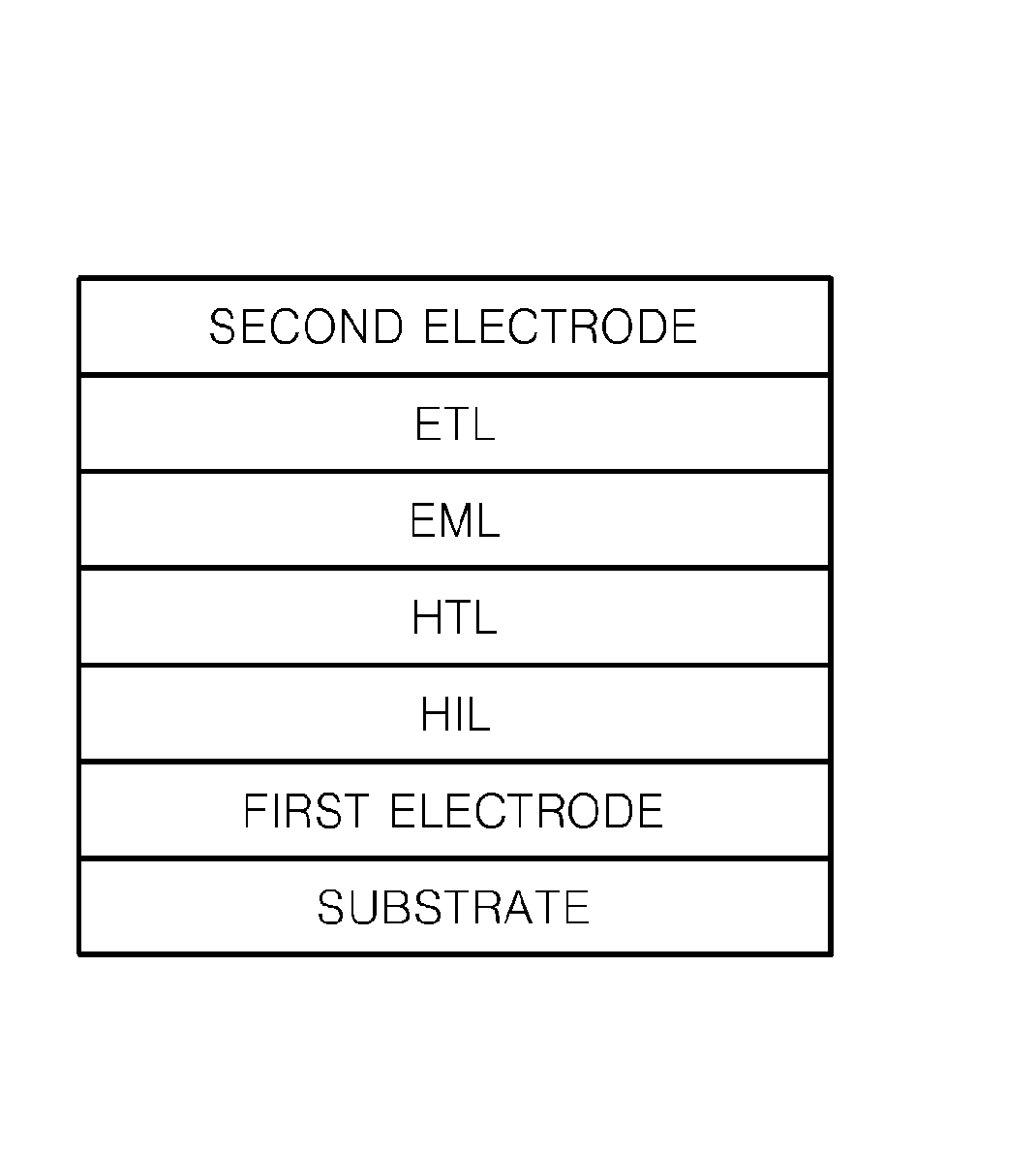
[0061]For the anode, a Corning 15 Ω / cm2 (1200 Å) ITO glass substrate was cut into a size of 50 mm×50 mm×0.7 mm and washed by sonicating in isopropyl alcohol and deionized water for 5 minutes each, and then treated with UV ozone for 30 minutes.

[0062]On the top surface of the substrate, an HIL having a thickness of 5 nm was formed using copper phthalocyanine (CuPc).

[0063]On top of the HIL, an HTL was formed at a thickness of 60 nm by vacuum-depositing N,N′-bis(α-naphthyl)-N,N′-diphenyl-4,4′-diamine (NPB). After forming the HTL as mentioned, an emission layer was formed on top of the HTL by vacuum-depositing 100 parts by weight of Alq3 as a host and 10 parts by weight of coumarin 6 as a dopant.

[0064]Then, an ETL having a thickness of 35 nm was formed by vacuum-depositing 25 parts by weight of LiF and 75 parts by weight of Bebq2 on top of the emission layer.

[0065]Production of the organic light emitting device is completed by vacuum-deposit...

example 2

Production of the Organic Light Emitting Device

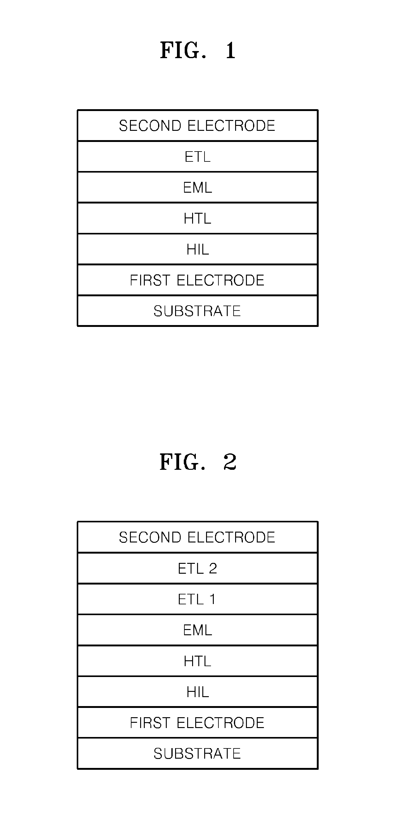
[0066]The organic light emitting device was produced in the same manner as in Example 1, except that the ETL was formed by vacuum-depositing 50 parts by weight of lithium quinolate and 50 parts by weight of Bebq2.

example 3

Production of the Organic Light Emitting Device

[0067]For the anode, a Corning 15 Ω / cm2 (1200 Å) ITO glass substrate was cut into a size of 50 mm×50 mm×0.7 mm and washed by sonicating in isopropyl alcohol and deionized water for 5 minutes each, and then washed in UV ozone for 30 minutes.

[0068]On the top surface of the substrate, an HIL having a thickness of 5 nm was formed using copper phthalocyanine (CuPc).

[0069]On top of the HIL, an HTL was formed at a thickness of 60 nm by vacuum-depositing NPB. After forming the HTL as mentioned, an emission layer was formed on top of the HTL by vacuum-depositing 100 parts by weight of Alq3 as a host and 10 parts by weight of coumarin 6 as a dopant.

[0070]Then, a first electron transport layer, ETL1, having a thickness of 10 nm was formed by vacuum-depositing Bebq2 on top of the emission layer.

[0071]A second electron transport layer, ETL2, having a thickness of 15 nm was formed by vacuum-depositing 25 parts by weight of LiF and 75 parts by weight ...


PUM


Abstract

An organic light emitting device includes an electron transport layer including an electron transport material and a metallic compound represented by Formula 1:
Formula 1:
XaYb
wherein X is an alkaline metal, an alkaline earth metal, or a transition metal, and Y is one of a Group 7 element and an organic group C1-C20, and a is an integer within the range of 1 to 3, and b is an integer within the range of 1 to 3.

Description

CROSS-REFERENCE TO RELATED APPLICATION[0001]This application claims the benefit of Korean Application No. 2007-116759, filed Nov. 15, 2007, in the Korean Intellectual Property Office, the disclosure of which is incorporated herein by reference.BACKGROUND OF THE INVENTION[0002]1. Field of the Invention[0003]Aspects of the present invention relate to an organic light emitting device, and more particularly, to an organic light emitting device with improved driving voltage, light-emitting efficiency and lifetime by enhancing the electron injection abilities by incorporating a novel material for forming an electron transport layer.[0004]2. Description of the Related Art[0005]Organic light-emitting devices are self-emissive display devices that have drawn a large amount of attention due to a wide viewing angle, superior contrast, and quick response time.[0006]An organic light emitting device typically comprises an anode, a cathode, and an organic light emitting layer between the anode and...

Claims


Application Information

Patent Timeline
Patent Type & Authority Applications(United States)
IPC IPC(8): H01L51/52
CPCH01L51/0073H01L51/0081H01L51/0092H01L2251/308H01L51/5052H01L51/5092H01L51/5048H10K85/6574H10K85/324H10K85/381H10K50/14H10K50/165H10K50/171H10K2102/103C09K11/06C09K11/55H05B33/20H10K50/00
Inventor SONG, WON-JUNSUNG, YEUN-JOOKIM, MU-HYUNKRISTAL, BORISYANG, NAM-CHOULCHANG, SEUNG-WOOKLEE, SUN-HEE
Owner SAMSUNG DISPLAY CO LTD
Why Eureka
Try Eureka