

Semiconductor device, power supply device, and information processing device
a technology of information processing device and semiconductor device, which is applied in the direction of pulse technique, dc-dc conversion, power conversion system, etc., can solve the problems of large circuit area, low efficiency, and parasitic diodes, so as to reduce the potential difference, prevent parasitic diodes, and increase the potential difference
- Summary
- Abstract
- Description
- Claims
- Application Information
AI Technical Summary
Benefits of technology
Problems solved by technology
Method used
Image

Examples
first embodiment
[0060]To begin with, the invention will be described.
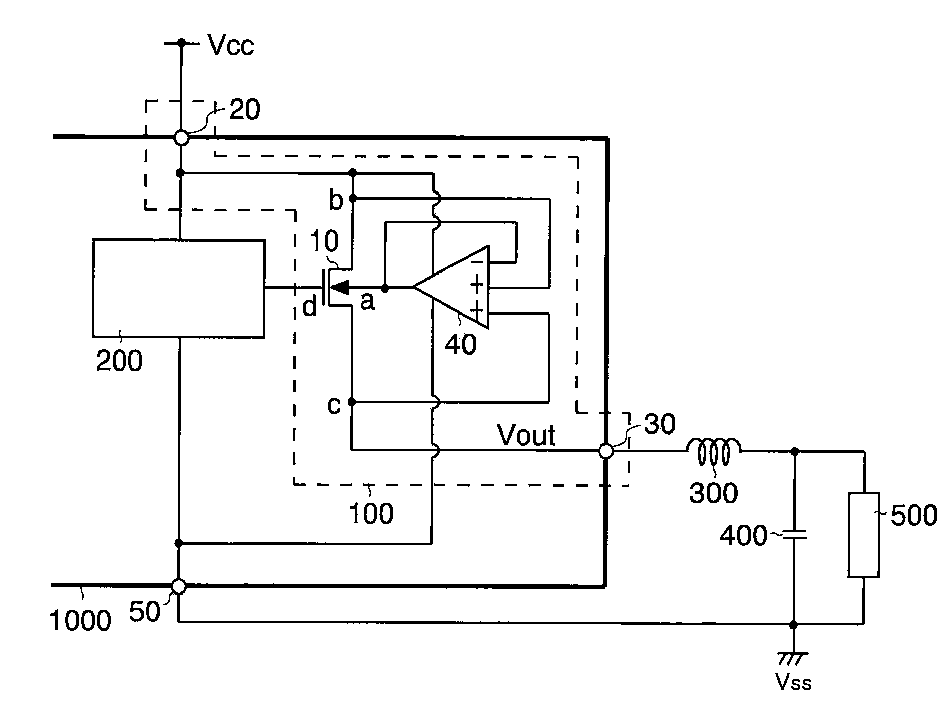
[0061]FIG. 1 is a diagram showing, as a first embodiment, a power supply device employing a semiconductor device according to the invention.
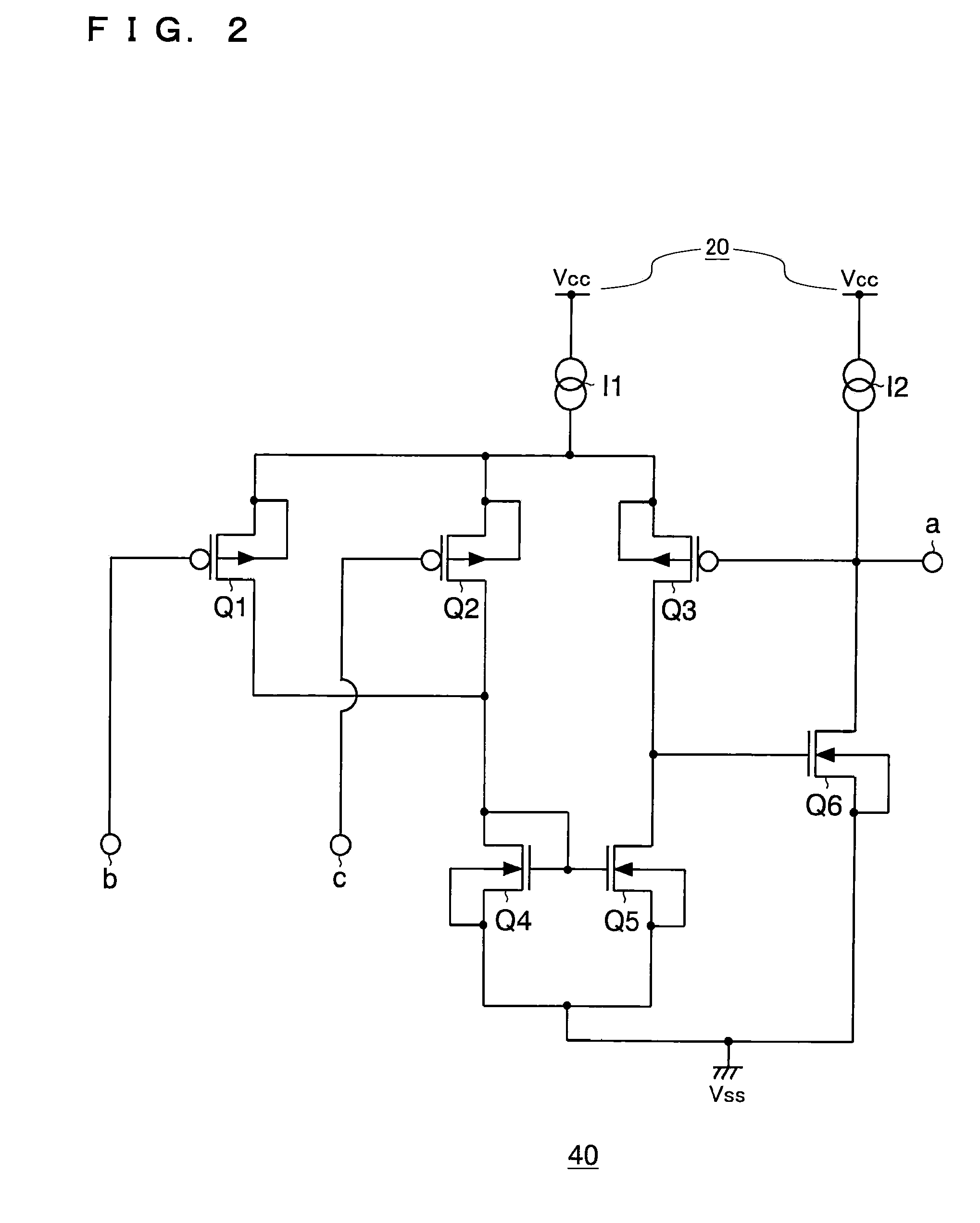
[0062]As shown in FIG. 1, the semiconductor device 100 of this embodiment forms part of a semiconductor device 1000. The semiconductor device 100 is composed of: a MOS transistor 10 having a backgate terminal “a”, a first region “b” serving as one of a source region and a drain region, and a second region “c” serving as the other of a source region and a drain region; an input terminal 20 that is connected to the first region “b” and to which, for example, a supply voltage Vcc is applied as an input voltage from outside the semiconductor device 1000; an output terminal 30 that is connected to the second region “c” and from which an output voltage Vout is outputted to outside the semiconductor device 1000; and a backgate control circuit 40 that applies either the input voltage Vcc or the output...
second embodiment
[0088]Next, the invention will be described.
[0089]FIG. 6 is a diagram showing, as a second embodiment, a power supply device employing a semiconductor device according to the invention.
[0090]As shown in FIG. 6, the semiconductor device 110 of this embodiment is composed of: a comparator 41 of which the non-inverting input terminal (+) is connected to the input terminal 20 and of which the inverting input terminal (−) is connected to the output terminal 30; an inverter circuit inv1 that receives the output of the comparator 41; a first switch SW1 that is opened and closed according to the output of the inverter circuit inv1, with a first end of the first switch SW1 connected to the input terminal 20 and a second end of the first switch SW1 connected to the backgate terminal “a” of the MOS transistor 10; and a second switch SW2 that is opened and closed according to the output of the comparator 41, with a first end of the second switch SW2 connected to the output terminal 30 and a sec...
third embodiment
[0097]Next, the invention will be described.
[0098]FIG. 7 is a diagram showing the configuration of an information processing device employing a semiconductor device according to the invention.
[0099]In FIG. 7, the reference numeral 710 represents an AC-DC (alternating current to direct current) conversion device, such as an AC adaptor, for producing a direct-current voltage (for example, 21 V) from alternating-current power distributed to households. The reference numeral 720 represents a secondary battery, that is, a rechargeable battery, using lithium, such as a lithium-polymer battery or a lithium-ion battery. The reference numeral 1000 represents a semiconductor device according to the invention like those previously described. The reference numeral 730 represents means for controlling an information processing device 7000 (such as a notebook personal computer), as typically realized in the form of a mother board 730. On the mother board 730, in addition to the semiconductor devi...
PUM
 Abstract
Description
Claims
Application Information