Master carrier for magnetic transfer and magnetic recording medium manufactured using the same
a technology of magnetic recording medium and master carrier, which is applied in the direction of data recording, instruments, coating parts of support with magnetic layers, etc., can solve the problems of difficult to provide a large difference in the intensity of transfer magnetic field between the patterns of projection and depression, difficult to saturate magnetically the layer of the master carrier, and deterioration of recorded signals in quality level, etc., to achieve favorable magnetic recording of signals, increase signal output, and high magnetic anisotropy energy
- Summary
- Abstract
- Description
- Claims
- Application Information
AI Technical Summary
Benefits of technology
Problems solved by technology
Method used
Image
Examples
example e-i
Preparation of Master Disc
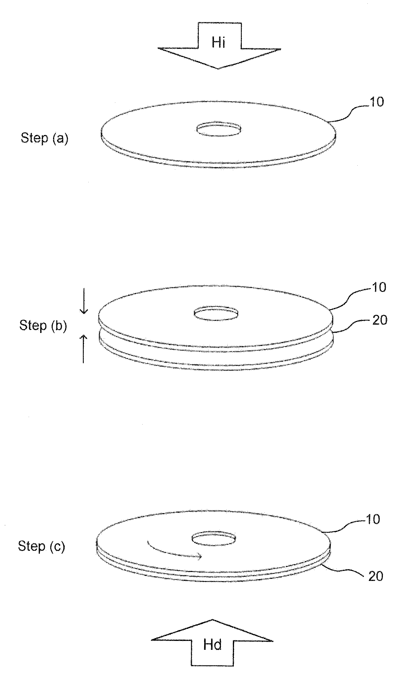
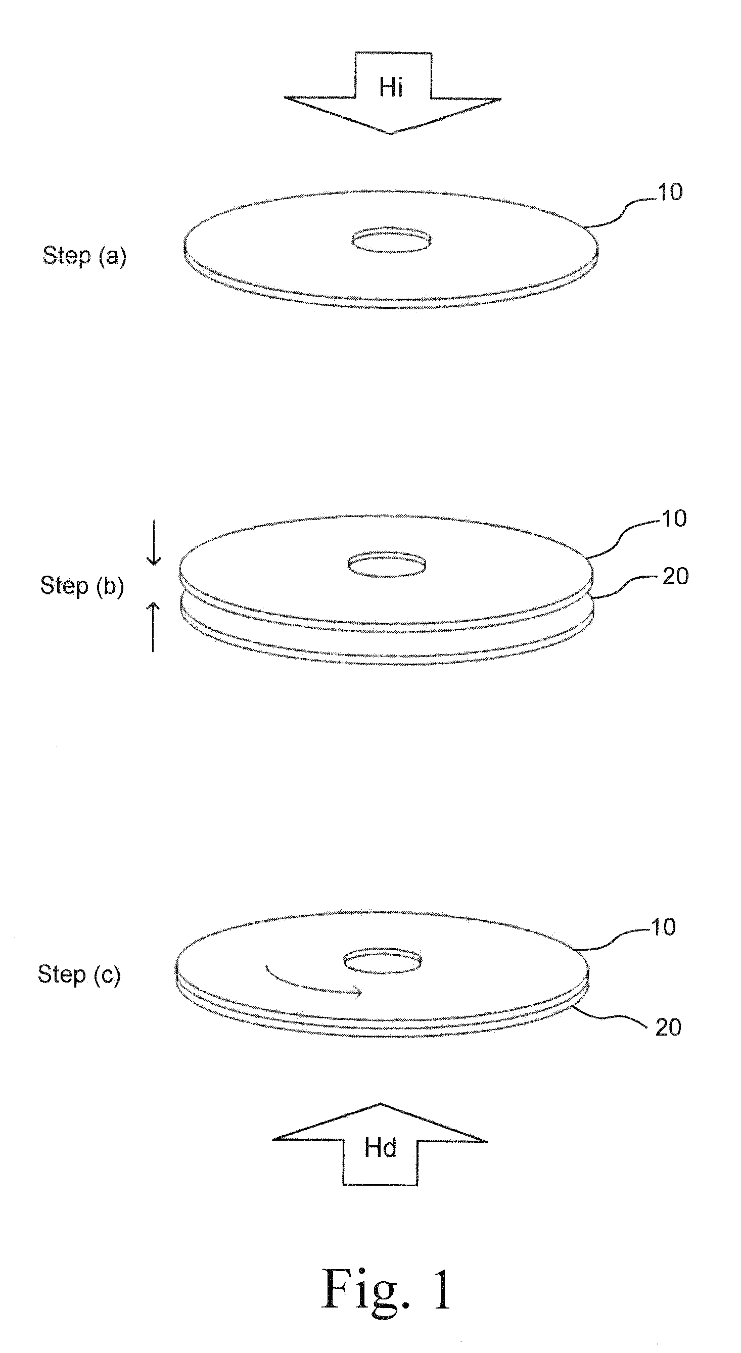
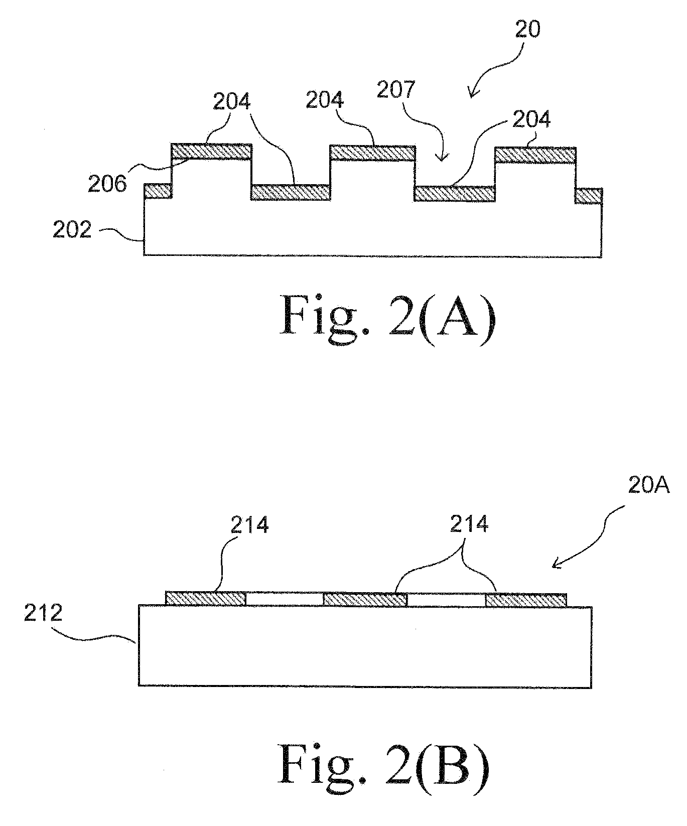
[0068]An electron beam resist coating layer was formed to a thickness of 100 nm on an 8-inch silicon wafer (base substrate) by spin coating. The resist layer was exposed to an electron beam by use of a rotary electron beam lithographic equipment and then developed to provide a patterned resist layer on the silicon wafer. The silicon wafer was processed by reactive ion beam etching using the patterned resist layer as a mask so as thereby to form a pattern of recesses in the silicon wafer and then washed to remove the patterned resist layer and dried. The recess-patterned silicon wafer was used as an original disc for preparing a master carrier 20.
(Fabrication of Master Carrier Intermediate)
[0069]A Ni electrical conductive layer was formed to a thickness of 20 nm on the original disc by sputtering. Then a Ni film was formed to a thickness of 200 μm by electrolytic plating the original disc with the Ni electrical conductive layer formed thereon dipped in an el...
example e-ii
[0075]A master carrier of example E-III was prepared by the same way as Example E-I except that a CoPt (Co: 88 atomic %; Pt: 12 atomic %) film was formed in place of the CoPt (Co: 80 atomic %; Pt: 20 atomic %) film. The magnetic layer of the master carrier had a magnetic anisotropy energy of 5.2×10⁶ erg / cm3 and a saturation magnetization of 1,260 emu / cc.
example e-iv
[0076]A master carrier of example E-IV was prepared by the same way as Example E-I, except that a Ta under layer and a magnetic layer were formed in an argon (Ar) gas atmosphere under a deposition pressure of 3.0 Pa. The magnetic layer of the master carrier had a magnetic anisotropy energy of 7.9×10⁶ erg / cm3 and a saturation magnetization of 930 emu / cc.
PUM
| Property | Measurement | Unit |
|---|---|---|
| thickness | aaaaa | aaaaa |
| thicknesses | aaaaa | aaaaa |
| thickness | aaaaa | aaaaa |
Abstract
Description
Claims
Application Information


