
Wavelength control in phase region of semiconductor lasers

a semiconductor laser and phase region technology, applied in semiconductor lasers, laser controllers, color television details, etc., can solve the problems of visible defects, output wavelength of semiconductor lasers moving outside of the allowable bandwidth,

Inactive Publication Date: 2009-05-21
CORNING INC
View PDF21 Cites 12 Cited by
  • Summary
  • Abstract
  • Description
  • Claims
  • Application Information

AI Technical Summary

Benefits of technology

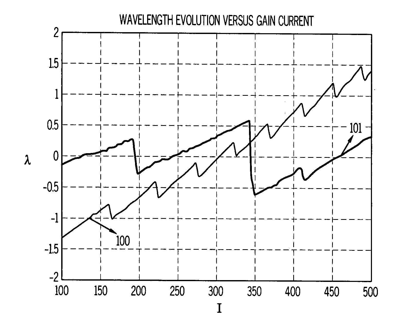
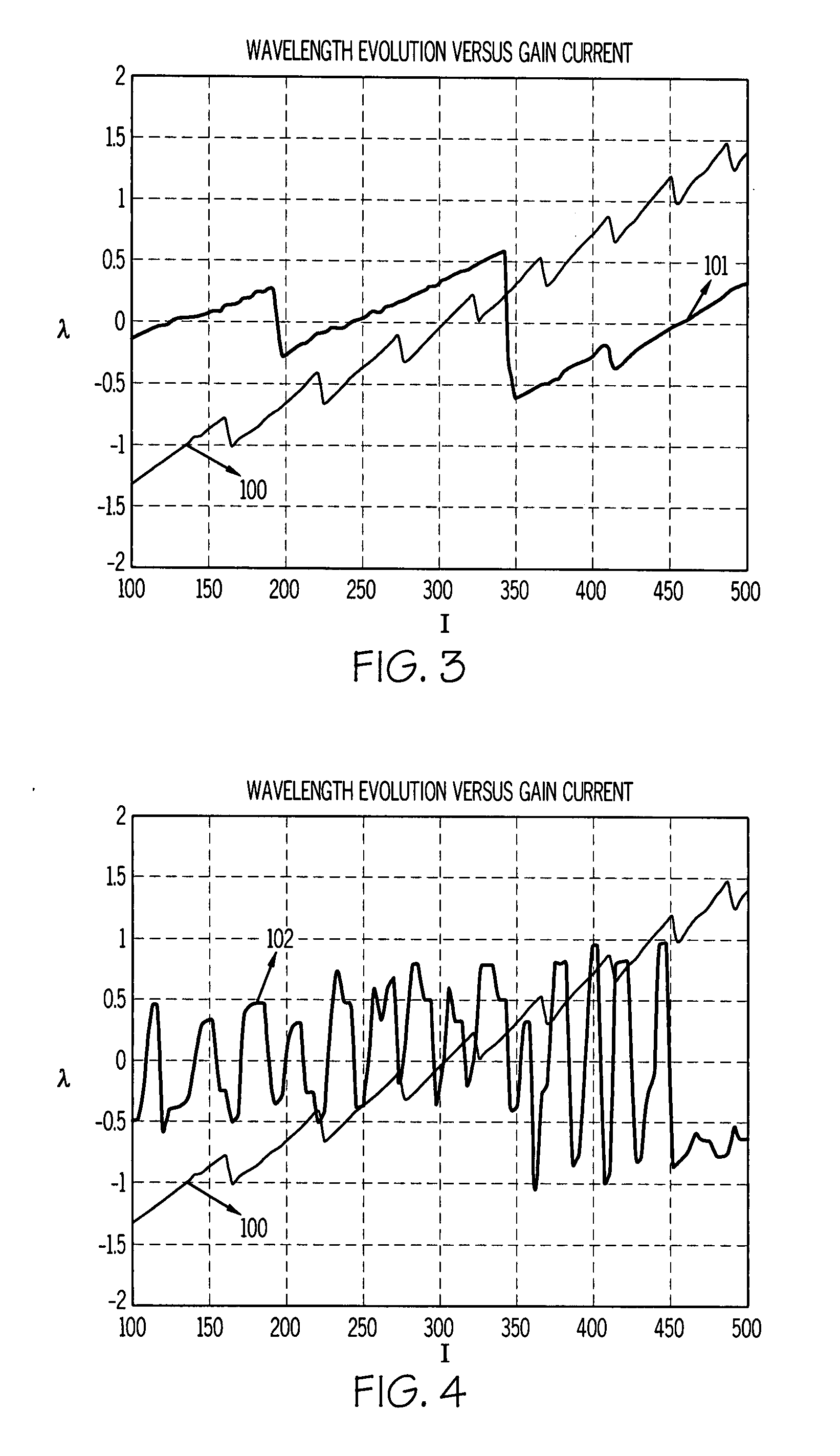
[0061]As an example, and not by way of limitation, when the cavity modes get close to the DBR wavelength, the wavelength oscillates between the highest power (the cavity modes aligned on the DRB curve) and the lowest power (cavity modes misaligned by one half of the free spectral range). Therefore, the fluctuation of the power averaged over two adjacent pixels gets reduced and any image defects are harder to detect. The present inventors have found that the fluctuation of power between pixels is reduced from 8% to 2%. Additionally, image noise, which is the standard deviation calculated for each pixel of the image over many identical image frames, was found to be around 7% when using some embodiments of the present invention. Another advantage of the present invention is that the wall plug efficiency of the laser is improved. By sending a square-wave signal into the phase section rather than providing a high current injection, the power applied to the phase section is reduced. For example and by illustration, not limitation, one embodiment of the present invention requires only 90 mW of power into the phase section.
[0062]Although the present invention has been described with primary reference to pixel-based projection systems, it is contemplated that other projection systems, such as spatial light modulator based systems (including digital light processing (DLP), transmissive LCD, and liquid crystal on silicon (LCOS)), incorporating laser-based light sources may benefit from the wavelength stabilization and perturbation techniques described herein. In these other systems the relevant period exogenous to the laser is not the pixel period but the inverse of the screen refresh rate, or a fraction thereof. In these cases the input signal to the laser will be characterized by an encoded data period tP and the drive current will be configured such that the recovery duration tR of the wavelength recovery portion is less than the encoded data period tP.
[0063]Reference is made throughout the present application to various types of currents. For the purposes of describing and defining the present invention, it is noted that such currents refer to electrical currents. Further, for the purposes of defining and describing the present invention, it is noted that reference herein to “control” of an electrical current does not necessarily imply that the current is actively controlled or controlled as a function of any reference value. Rather, it is contemplated that an electrical current could be controlled by merely establishing the magnitude of the current.

Problems solved by technology

Mode hopping and uncontrolled large wavelength variations within the laser cavity can cause the output wavelength of a semiconductor laser to move outside of this allowable bandwidth during operation.
In laser projection systems, for example, mode hops are particularly problematic because they can generate instantaneous changes in power that will be readily visible as defects at specific locations in the image.
These visible defects typically manifest themselves as organized, patterned image defects across the image because the generated image is simply the signature of the temperature evolution of the different sections of the laser.

Method used


Image

  • Wavelength control in phase region of semiconductor lasers
  • Wavelength control in phase region of semiconductor lasers
  • Wavelength control in phase region of semiconductor lasers

Examples


Embodiment Construction

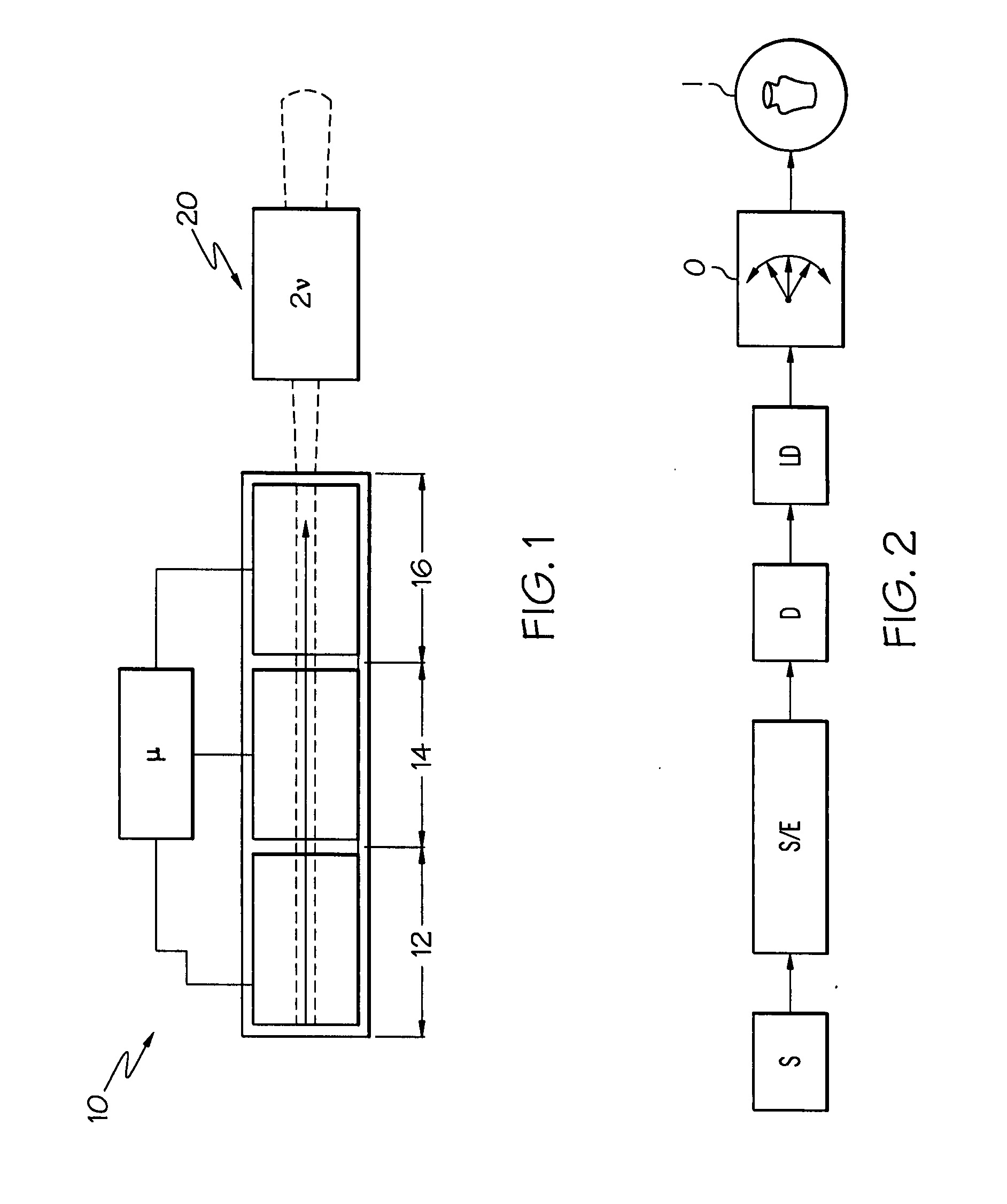
[0020]Although the specific structure of the various types of semiconductor lasers in which the concepts of particular embodiments of the present invention can be incorporated is taught in readily available technical literature relating to the design and fabrication of semiconductor lasers, the concepts of particular embodiments of the present invention may be conveniently illustrated with general reference to a three-section DBR-type semiconductor laser 10 illustrated schematically in FIG. 1. In FIG. 1, the DBR laser 10 is optically coupled to a light wavelength conversion device 20. The light beam emitted by the semiconductor laser 10 can be either directly coupled into the waveguide of the wavelength conversion device 20 or can be coupled through collimating and focusing optics or some other type of suitable optical element or optical system. The wavelength conversion device 20 converts the incident light into higher harmonic waves and outputs the converted signal. This type of c...


PUM


Abstract

Particular embodiments of the present invention relate generally to semiconductor lasers and laser scanning systems and, more particularly, to schemes for controlling semiconductor lasers. According to one embodiment of the present invention, a laser is configured for optical emission of encoded data. At least one parameter of the optical emission is a function of a drive current IGAIN injected into the gain section of the semiconductor laser and one or more additional drive currents I / VPHASE, I / VDBR. Mode selection in the semiconductor laser is altered by applying a phase shifting signal I / VΦ to the phase section that is synched with a wavelength recovery portions in drive current IGAIN such that a plurality of cavity modes are shifted by one half of the free spectral range at each wavelength recovery portion. In this manner, patterned variations in the wavelength or intensity profile of the laser can be disrupted to disguise patterned flaws that would otherwise be readily noticeable in the output of the laser.

Description

BACKGROUND OF THE INVENTION[0001]The present invention relates generally to semiconductor lasers, laser controllers, laser projection systems, and other optical systems incorporating semiconductor lasers. More particularly, some embodiments of the present invention relate to schemes for managing laser wavelength variations in semiconductor lasers. Other embodiments of the present invention relate to schemes for minimizing systematic wavelength variations in the output of a wavelength conversion device optically coupled to a semiconductor laser, and schemes for disrupting the temperature evolution signature within a scanned laser image of a laser projection system.SUMMARY OF THE INVENTION[0002]The present invention relates generally to semiconductor lasers, which may be configured in a variety of ways. For example and by way of illustration, not limitation, short wavelength sources can be configured for high-speed modulation by combining a single-wavelength semiconductor laser, such ...

Claims


Application Information

Patent Timeline
Patent Type & Authority Applications(United States)
IPC IPC(8): H01S3/10
CPCH01S5/005H01S5/0092H01S5/06246H04N9/3158H01S5/06832H01S5/0687H04N9/3129H01S5/06256
Inventor GOLLIER, JACQUES
Owner CORNING INC
Learn More