Defect review method and apparatus

Active Publication Date: 2009-05-28
HITACHI HIGH-TECH CORP
View PDF9 Cites 64 Cited by
  • Summary
  • Abstract
  • Description
  • Claims
  • Application Information

AI Technical Summary

Benefits of technology

[0015]The present invention is to solve the problems described above and is to provide a defe

Problems solved by technology

However, in recent years, as pattern integration has progressed, it has become difficult to form a fine mask pattern shape with fidelity on a wafer by use of the optical exposure method.
This is because, when the pattern shape defect is caused due to the pattern failure as described above, there is a high probability that the defect is critical for the device, such that the pattern shape defect that can occurs with fluctuation in process condition has to be monitored.
In a semiconductor device manufacturing line, there also occur random defects whose defect occurrence position is not dependent on the circuit pattern.
Even such a random defect can be a cause of reducing the production yield, such that a countermeasure therefor is necessary.
Hence, in many cases, while the presence of a defect can be evaluated from a detected low resolution image, the type of the defect cannot be determined therefrom.
However, as integrat

Method used


Image

  • Defect review method and apparatus
  • Defect review method and apparatus
  • Defect review method and apparatus

Examples


Example

First Embodiment

[0066]A first embodiment of the present invention will be described herebelow.

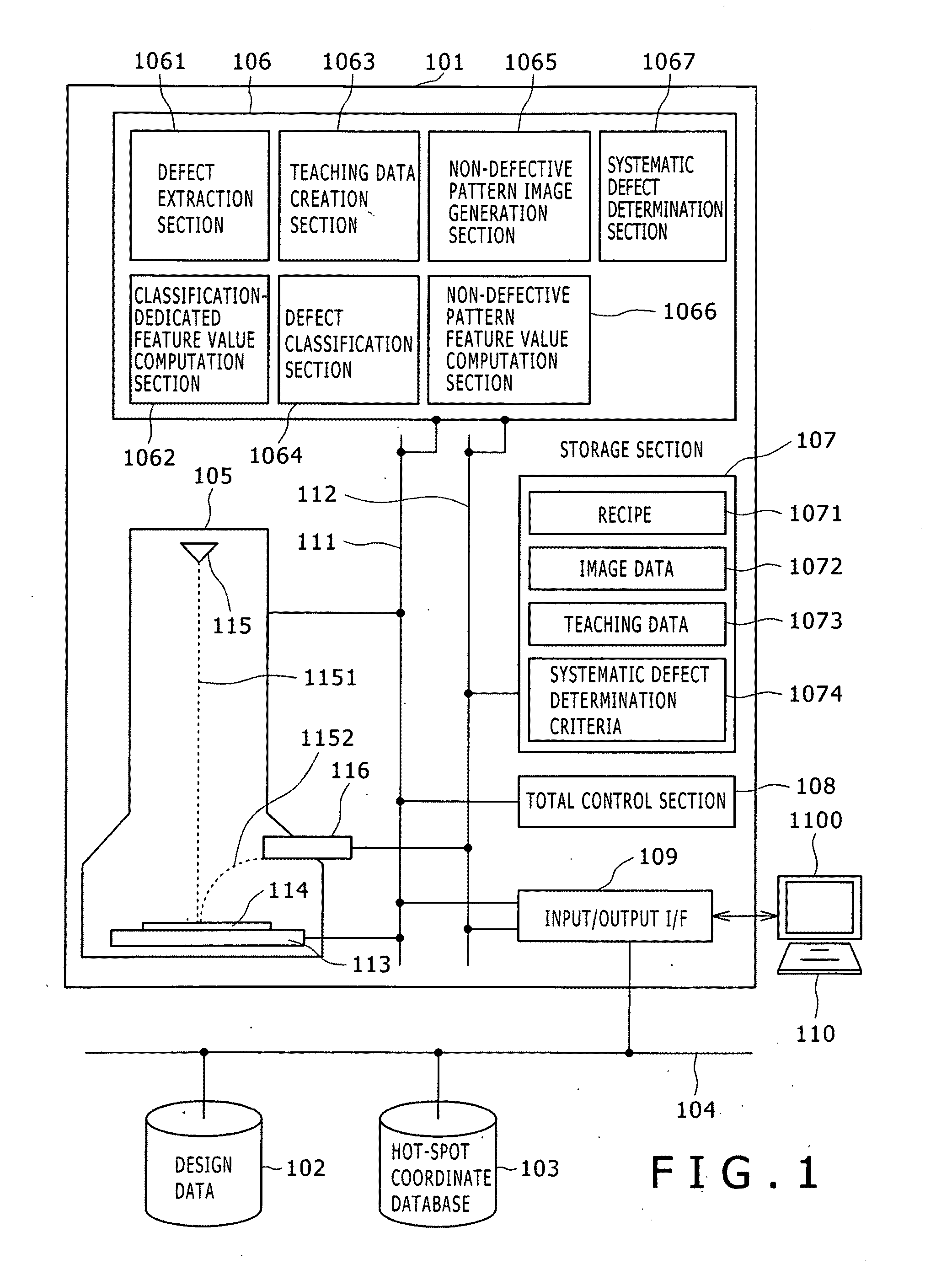
[0067]FIG. 1 is a view showing the configuration of a system for executing the defect review method according to the present invention. A review SEM 101 is configured to include an electronic optical system 105 that acquire electronic microscope images; a processor and analyzer section 106 that executes various processes; a storage section 107 that stores various data therein; an input / output I / F 109 (I / F=interface) that performs data input or output in communication with the outside, and a total control section 108 that controls the respective sections. The respective sections are interconnected via a control bus 111 and a data bus 112. The input / output I / F 109 is connected to an input / output terminal 110, such as a display / keyboard. An operator is enabled to issue instructions or commands or to verify the apparatus status via the input / output terminal 110.

[0068]In the electronic optical s...

Example

Second Embodiment

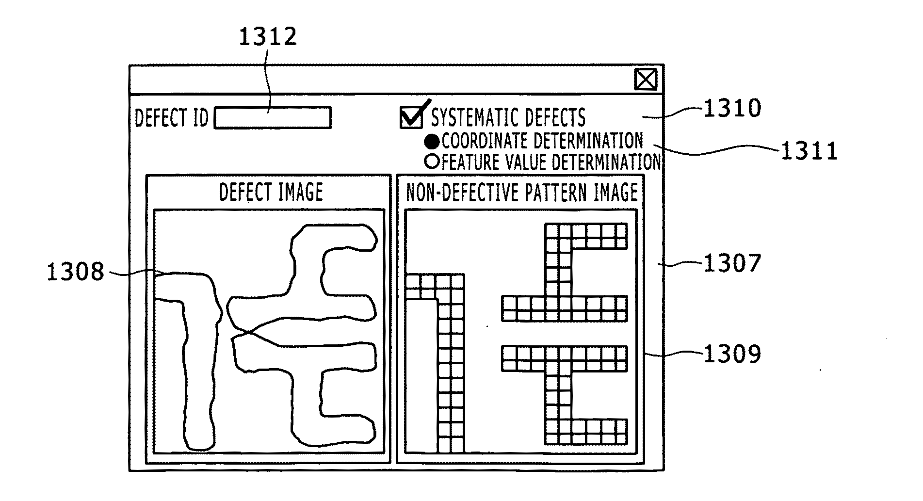
[0124]A defect review method of a second embodiment of the present invention will be described herebelow. A system configuration as used in the present, second embodiment is identical to that shown in FIG. 1. According to the first embodiment, the non-defective pattern image, which is used for specifying the systematic defect determination criteria as the image data 1072 stored in the storage section 107, is created by use of the coordinate data stored in the hot-spot coordinate database 103. According to the present embodiment, however, the process is characterized in that the defect classification result is utilized for the creation of the non-defective pattern image, thereby to redefine the systematic defect determination criteria 1074. More specifically, as a result of the execution of the process shown in FIG. 3, the classification results and the systematic defect determination results are obtained in respective defect image datasets. The classification result...


PUM


Abstract

A candidate-defect classification method includes the steps of acquiring a scanning electron microscope (SEM) image of a candidate defect detected in an inspection from a sample including a pattern formed thereon, the inspection being preliminarily performed by an other inspection device; computing a feature value of the candidate defect by processing the SEM image; executing defect classification of the candidate defect as any one of a pattern shape defect and an other defect by using the computed feature value; acquiring positional information contained in design data of the pattern with respect to a candidate defect classified as the pattern shape defect; and extracting a systematic defect from among candidate defects classified as the pattern shape defects by performing a comparison of the positional information contained in the design data of the acquired candidate defect to positional information of a portion that has a high probability of causing a pattern formation failure and that has been obtained from the design data of the pattern, the systematic defect being caused due to a layout shape of the pattern, properties of a processor for forming the pattern, or the like.

Description

CLAIM OF PRIORITY[0001]The present application claims priority from Japanese application serial no. JP2007-295036, filed on Nov. 14, 2007, the content of which is hereby incorporated by reference into this application.BACKGROUND OF THE INVENTION[0002]The present invention relates to a defect review method and apparatus for reviewing and classifying an image of a defect or the like occurring during manufacturing processes of a semiconductor wafer or the like.[0003]Conventionally, in semiconductor wafer manufacture, an optical exposure process or method has been adapted as a circuit pattern transfer method. However, in recent years, as pattern integration has progressed, it has become difficult to form a fine mask pattern shape with fidelity on a wafer by use of the optical exposure method. As such, a method called “OPC” (optical proximity correction) has been widely used. Among other things, OPC is used to perform operations on integrated mask patterns, such as preliminarily addition...

Claims


Application Information

Patent Timeline
IPC IPC(8): G06T7/00
CPCG06T7/0006G06T7/001G06T2207/30148G06T2207/10061
Inventor NAKAGAKI, RYOHARADA, MINORUHIRAI, TAKEHIRO
Owner HITACHI HIGH-TECH CORP
Why Eureka
Try Eureka