Reduced Leakage Driver Circuit and Memory Device Employing Same

a memory device and leakage current technology, applied in the field of semiconductor memory devices, can solve the problems of increasing the size of the driver, affecting and contributing to the standby power consumption of the memory device, so as to reduce the leakage current, increase the size or degrade the performance of the circuit.

Active Publication Date: 2009-06-04
AVAGO TECH INT SALES PTE LTD
View PDF1 Cites 27 Cited by
  • Summary
  • Abstract
  • Description
  • Claims
  • Application Information

AI Technical Summary

Benefits of technology

[0006]Illustrative embodiments of the present invention meet the above-noted need by providing an enhanced row line driver circuit having reduced leakage current compared to standard row line driver circuits without significantly increasing a size or degrading performance of the circuit. To accomplish this, a driver circuit in accordance with an illustrative embodiment of the invention is advantageously operative to allow a corresponding row line to which the driver circuit is connected to float during at least an inactive phase of a given memory cycle.

Problems solved by technology

Leakage current in memory devices contributes significantly to standby power consumption in the memory devices.
For even moderate size memory arrays, the load presented by a row line can be quite large, thereby requiring large drivers in order to achieve reasonable memory access times. Unfortunately, leakage current in the driver generally increases with the size of the driver.
Moreover, as semiconductor device geometries shrink, leakage current in these devices increases, thereby exacerbating the problem.
This approach, however, results in slower memory performance due primarily to increasing rise and / or fall times of the row lines.
As a result, it takes a significant amount of time for the intermediate node to equalize to a low-current state following a row line access, which is undesirable.

Method used


Image

  • Reduced Leakage Driver Circuit and Memory Device Employing Same
  • Reduced Leakage Driver Circuit and Memory Device Employing Same
  • Reduced Leakage Driver Circuit and Memory Device Employing Same

Examples


Embodiment Construction

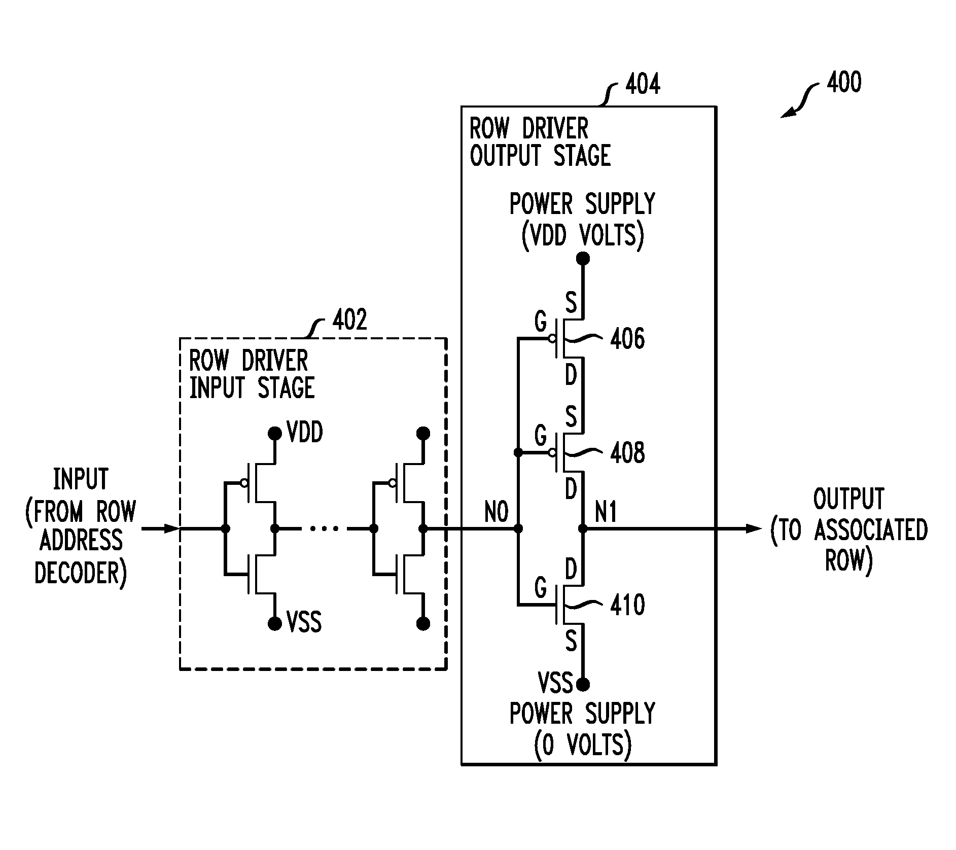
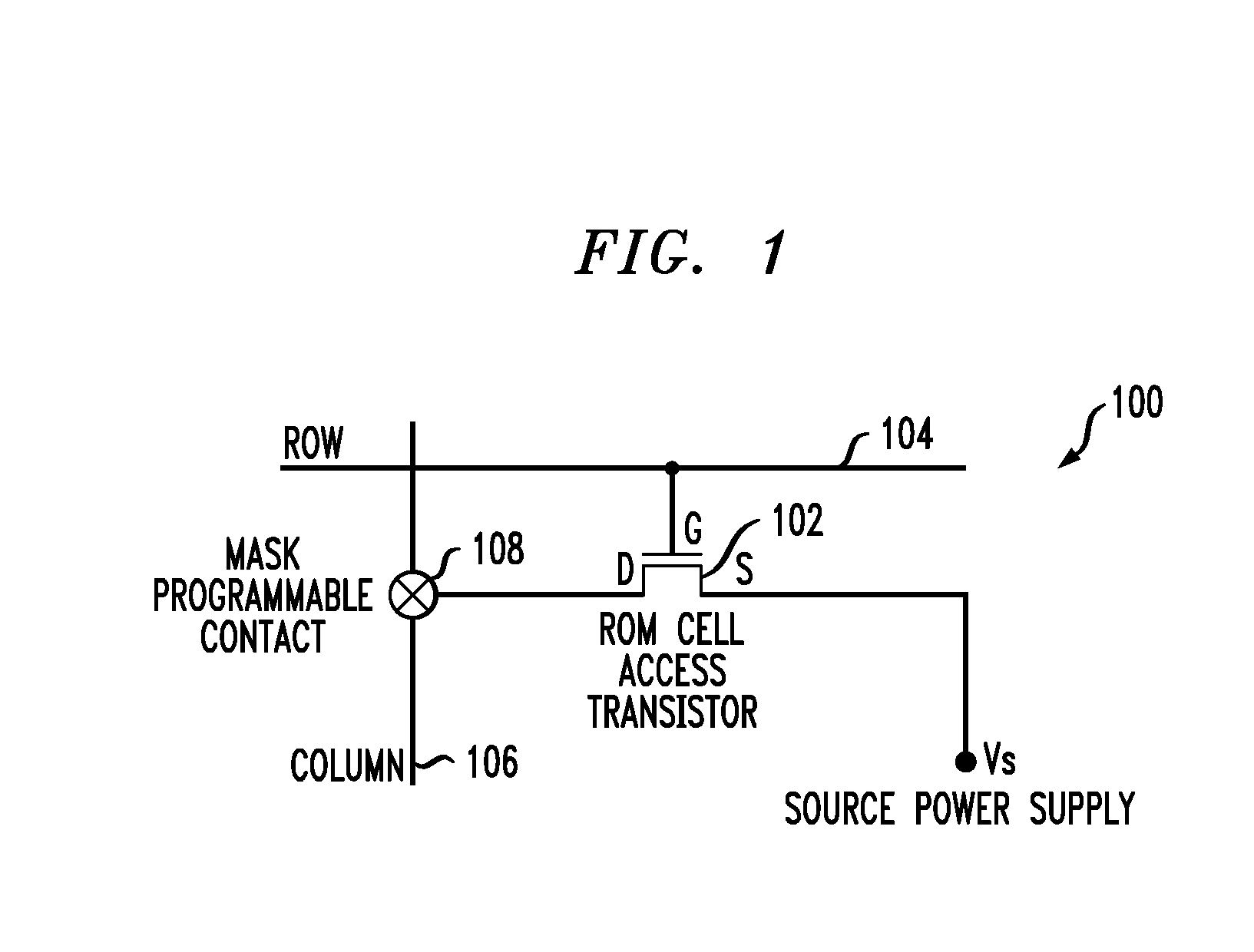
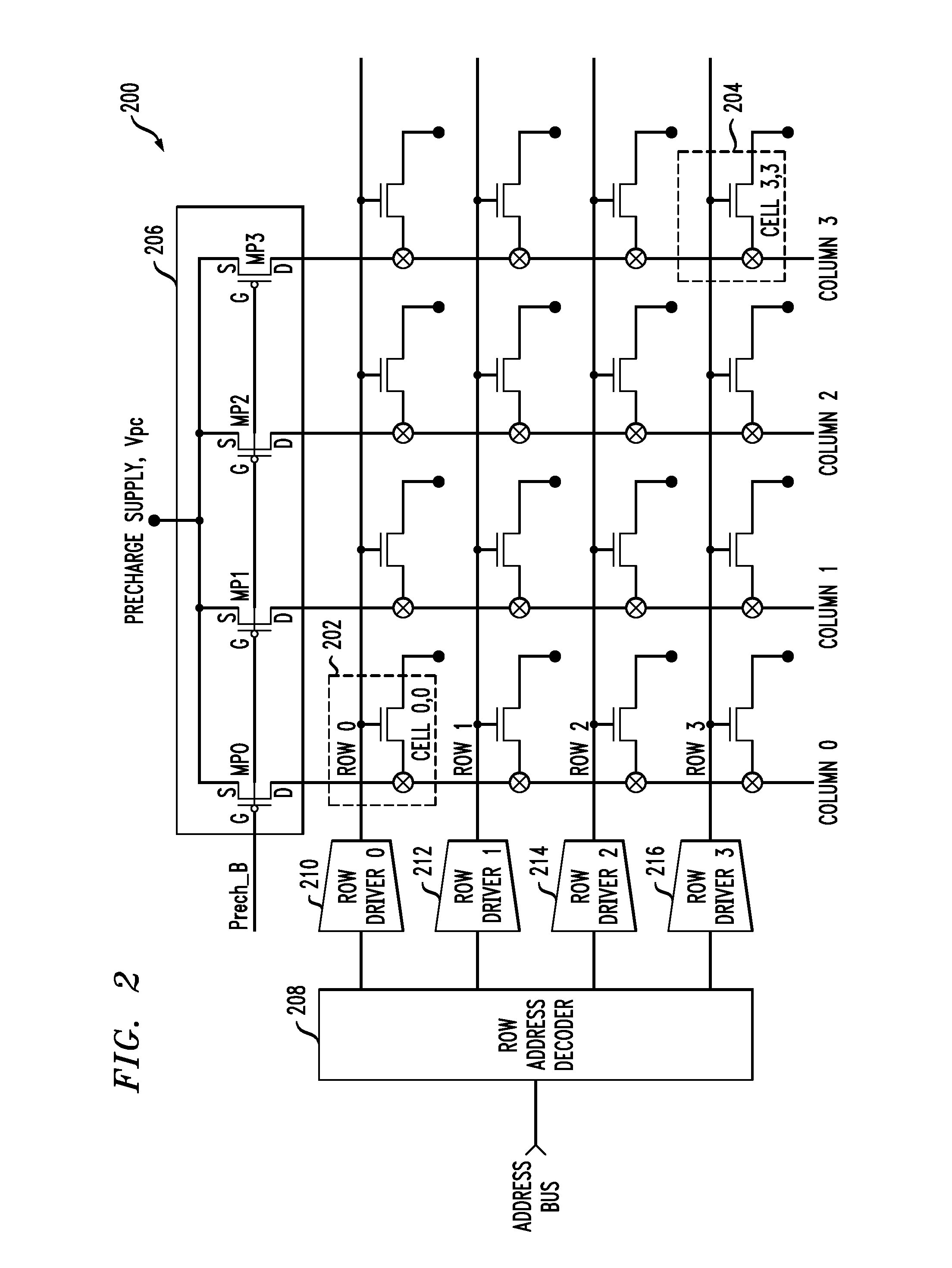
[0019]The present invention will be described herein in the context of exemplary methods and circuits for reducing leakage current in an embedded memory in an IC device. It is to be understood, however, that the techniques of the present invention are not limited to the methods and circuits shown and described herein. Rather, embodiments of the invention are directed to techniques for reducing the overall power consumption in a semiconductor memory device by reducing leakage current in one or more row line driver circuits in the memory device without significantly impacting performance and / or area.

[0020]A “device” as the term is used herein is intended to be broadly construed so as to encompass, by way of example only and without limitation, elements such as those commonly associated with an application-specific integrated circuit (ASIC), single inline memory module (SIMM), dual inline memory module (DIMM), content-addressable memory (CAM), central processing unit (CPU), digital sig...


PUM


Abstract

A row line driver circuit for use in a memory array including multiple memory cells and multiple row lines coupled to the memory cells for selectively accessing the memory cells includes an output stage adapted for connection to a corresponding one of the row lines and a control circuit connected to the output stage. The output stage is operative during an active phase of a given memory cycle to drive the corresponding row line to a potential as a function of at least one address signal received by the driver circuit. The control circuit is operative to generate at least one control signal for disabling the output stage at least during an inactive phase of the memory cycle to thereby substantially eliminate a leakage current path in the driver circuit.

Description

FIELD OF THE INVENTION[0001]The present invention relates generally to the electrical, electronic, and computer arts, and more particularly relates to semiconductor memory devices.BACKGROUND OF THE INVENTION[0002]Reducing power consumption in memory devices is becoming more important, particularly in view of their growing use in mobile applications and devices, including, for example, cell phones, handheld computing devices (e.g., Blackberry® devices, a registered trademark of Research in Motion Limited), MP3 players (e.g., ipod®, a registered trademark of Apple Inc.), global positioning system (GPS) instruments, laptop and palmtop computers, etc. Leakage current in memory devices contributes significantly to standby power consumption in the memory devices. For instance, in a memory array (e.g., read only memory (ROM)) which includes a plurality of column lines and row lines, with associated row line drivers, for selectively reading one or more memory cells in the memory array, the ...

Claims


Application Information

Patent Timeline
Patent Type & Authority Applications(United States)
IPC IPC(8): G11C8/00
CPCG11C8/08
Inventor EVANS, DONALD ALBERTMCPARTLAND, RICHARD J.PHAM, HAI QUANGWERNER, WAYNE E.WOZNIAK, RONALD JAMES
Owner AVAGO TECH INT SALES PTE LTD
Why Eureka
Try Eureka