Evaporation Donor Substrate and Method for Manufacturing Light-Emitting Device

a donor substrate and light-emitting technology, applied in the direction of solid-state devices, metallic material coating processes, synthetic resin layered products, etc., can solve the problem of inaccurate formation of el layers, achieve excellent characteristics, reduce manufacturing costs of light-emitting devices, and increase accuracy of patterning of el layers

Active Publication Date: 2009-06-04
SEMICON ENERGY LAB CO LTD
View PDF29 Cites 39 Cited by
  • Summary
  • Abstract
  • Description
  • Claims
  • Application Information

AI Technical Summary

Benefits of technology

[0026]According to the present invention, accuracy of patterning of an EL layer is heightened in formation of the EL layer over a deposition target substrate. Accordingly, a lig...

Problems solved by technology

In addition, the blocking mask which is irradiated with laser light is expanded by...

Method used


Image

  • Evaporation Donor Substrate and Method for Manufacturing Light-Emitting Device
  • Evaporation Donor Substrate and Method for Manufacturing Light-Emitting Device
  • Evaporation Donor Substrate and Method for Manufacturing Light-Emitting Device

Examples


embodiment mode 1

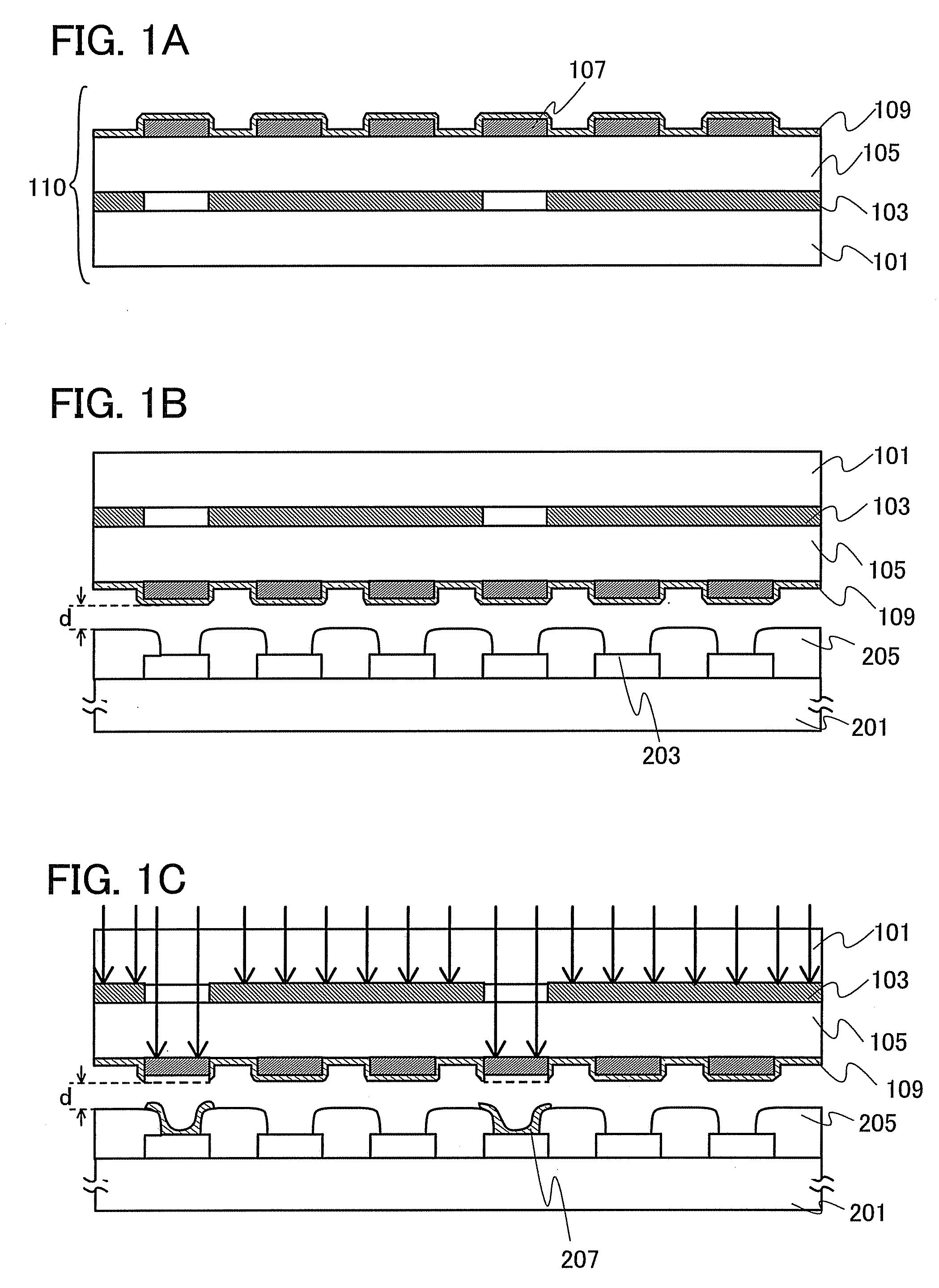
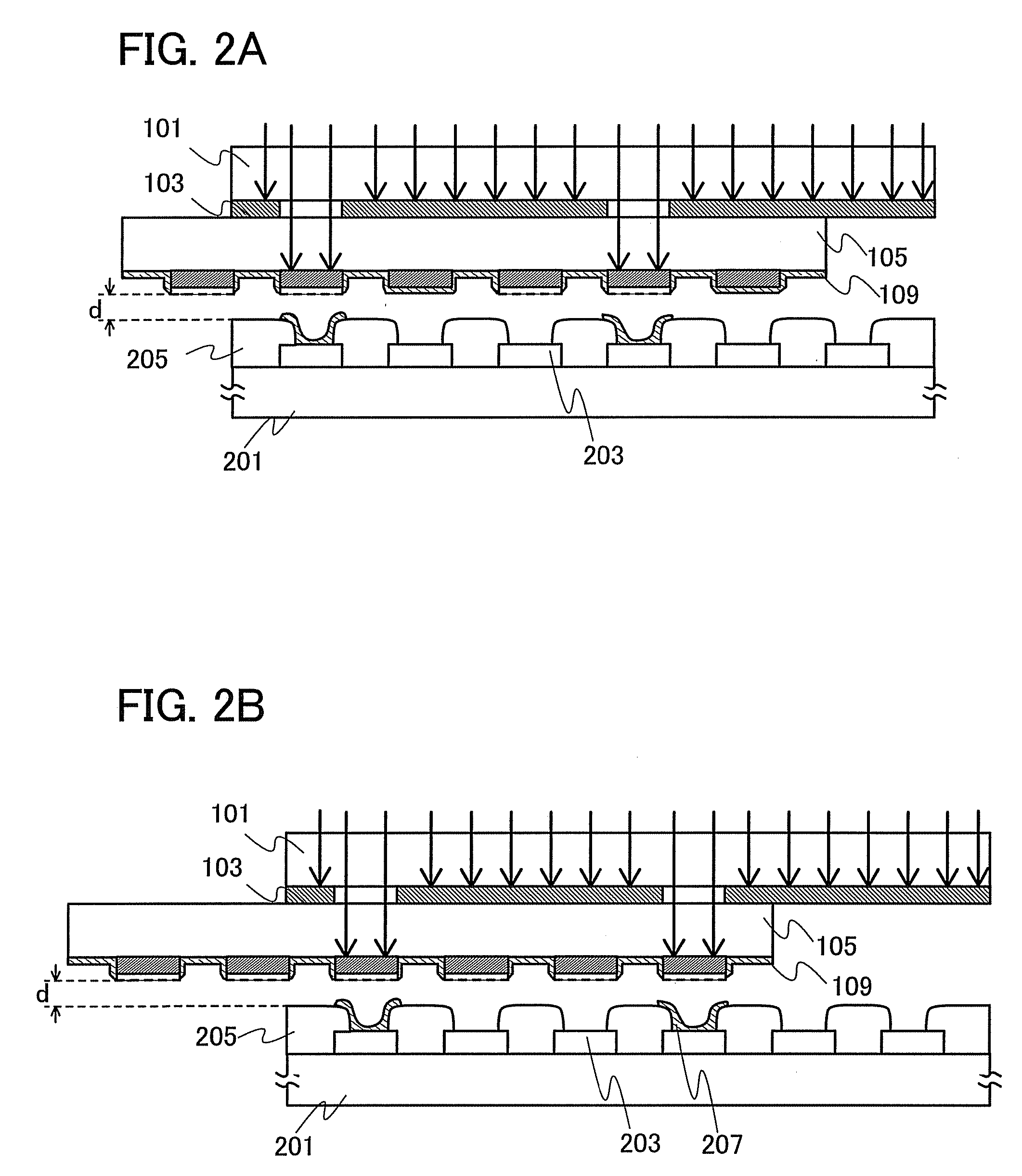
[0044]An evaporation donor substrate and a method for manufacturing a light-emitting device according to the present invention are described with reference to FIGS. 1A to 1C and FIGS. 2A and 2B.

[0045]FIG. 1A illustrates an evaporation donor substrate 110 according to the present invention. In FIG. 1A, a reflective layer 103 is formed on a surface of a first supporting substrate 101. The reflective layer 103 includes island-shaped or stripe-shaped openings. In addition, the reflective layer 103 and a second supporting substrate 105 are disposed so that the reflective layer 103 and a back surface of the second supporting substrate 105 are in contact with each other. A light absorption layer 107 which is patterned into island or stripe shapes is formed on a front surface of the second supporting substrate 105. In addition, a material layer 109 is formed over the light absorption layer 107. In FIG. 1A, the material layer 109 is formed so as to cover the entire surface of the second supp...

embodiment mode 2

[0101]This embodiment mode describes a method for manufacturing a full-color display device by using the evaporation donor substrate described in the above embodiment mode.

[0102]Embodiment Mode 1 describes an example in which an EL layer of single color is formed in every three pixels using one evaporation donor substrate. However, in the case of manufacturing a full-color display device, light-emitting layers for emitting light of different colors are formed in different regions through a plurality of deposition steps.

[0103]A manufacturing example of a light-emitting device capable of full-color display is described below. Here, a light-emitting device using light-emitting layers for emitting light of three colors is given as an example.

[0104]Three evaporation donor substrates illustrated in FIG. 1A are prepared. In each of the evaporation donor substrates, a material layer containing a different kind of evaporation material is formed. Specifically, a first evaporation donor substr...

embodiment mode 3

[0120]In this embodiment mode, examples of deposition apparatuses which enable manufacture of the light-emitting device of the present invention are described. FIGS. 5A and 5B and FIGS. 6A and 6B are schematic cross-sectional views of deposition apparatuses of this embodiment mode.

[0121]In FIG. 5A, a deposition chamber 801 is a vacuum chamber and is connected to other treatment chambers via a first gate valve 802 and a second gate valve 803. In addition, the deposition chamber 801 includes at least an evaporation donor substrate supporting mechanism which is an evaporation donor substrata supporting means 804, a deposition target substrate supporting mechanism which is a deposition target substrate supporting means 805, and a light source 810.

[0122]First, in another deposition chamber, with the structure described in the above embodiment mode, a material layer 808 is formed over the second supporting substrate provided with a light absorption layer. In this embodiment mode, the evap...


PUM

PropertyMeasurementUnit
Thicknessaaaaaaaaaa
Thicknessaaaaaaaaaa
Thicknessaaaaaaaaaa

Abstract

A first supporting substrate on a front surface of which a reflective layer having an opening is formed and a second supporting substrate on a front surface of which a light absorption layer patterned into island or stripe shapes and a material layer over the light absorption layer are formed are prepared, the first and second supporting substrates are disposed so that the opening of the reflective layer and the light absorption layer overlap with each other and the reflective layer is in contact with a back surface of the second supporting substrate, the second supporting substrate and a deposition target substrate are disposed so that the front surface of the second supporting substrate faces the deposition target substrate, and the material layer is attached to the deposition target substrate by irradiating the back surface of the first supporting substrate with light and by sublimating the material layer.

Description

BACKGROUND OF THE INVENTION[0001]1. Field of the Invention[0002]The present invention relates to light-emitting devices and methods of manufacturing the light-emitting devices. The present invention also relates to evaporation donor substrates which are used for deposition of a material which can be deposited onto a substrate.[0003]2. Description of the Related Art[0004]Organic compounds can take various structures compared with inorganic compounds, and it is possible to synthesize materials having various functions by appropriate molecular design. Because of these advantages, photo electronics and electronics which utilize functional organic materials have been attracting attention in recent years.[0005]Solar cells, light-emitting elements, organic transistors, and the like are given as examples of electronics devices using an organic compound as a functional organic material. These devices take advantage of electrical properties and optical properties of the organic compound. Amon...

Claims


Application Information

Patent Timeline
IPC IPC(8): B05D5/06B32B3/10
CPCB32B3/10Y10T428/24339B32B7/12B32B15/043B32B15/08B32B27/281B32B27/304B32B27/308B32B27/34B32B27/36B32B3/12B32B3/30B32B2262/101B32B2307/206B32B2307/416B32B2457/20H01L51/0013C23C14/048H10K71/18H05B33/10H10K71/00
Inventor TAKAHASHI, RENASATO, YOSUKEYOKOHAMA, KOHEIAOYAMA, TOMOYA
Owner SEMICON ENERGY LAB CO LTD
Why Eureka
Try Eureka