Magnetic memory device having a C-shaped structure and method of manufacturing the same

a magnetic memory and c-shaped technology, applied in the field of memory devices, can solve the problems of limiting the endurance of erase/write cycles, causing catastrophic breakdown, and relatively long required charging time, and the order of 1 ms

Inactive Publication Date: 2009-06-11
MICROMEM TECH
View PDF5 Cites 55 Cited by
  • Summary
  • Abstract
  • Description
  • Claims
  • Application Information

AI Technical Summary

Benefits of technology

[0012]Another object of the present invention is to provide a simplified method of fabricating a non-volatile magnetic memory device.

Problems solved by technology

One serious limitation to this technology is related to tunneling that limits the erase / write cycle endurance and can induce catastrophic breakdown (after a maximum of about 106 cycles).
Moreover, the required charging time—which is of the order of 1 ms—is relatively long.
However, the need for an additional cycle to return a given bit to its original state for reading purposes aggravates the problems of dielectric fatigue.
This, in turn, is characterized by degradation in the ability to polarize the material.
Finally, fabrication process uniformity and control still remains a challenge.
The GMR structures showed a magnetoresistance of about 6%, but the exchange between the magnetic layers limited how quickly the magnetization could change direction.
Moreover magnetization curling from the edge of the strip imposed a limitation on the reduction in the cell size, or scaling.
PSV structures are amenable to scaling but the reported fields required to switch the hard magnetic layer are still too high for high density integrated circuits.
However, controlling the resistance uniformity (i.e., the tunneling barrier thickness and quality), and hence controlling the switching behavior from bit to bit remains a real challenge that has yet to be overcome in practical implementation.

Method used


Image

  • Magnetic memory device having a C-shaped structure and method of manufacturing the same
  • Magnetic memory device having a C-shaped structure and method of manufacturing the same
  • Magnetic memory device having a C-shaped structure and method of manufacturing the same

Examples


Embodiment Construction

[0028]Reference will now be made in detail to the preferred embodiments of the present invention, examples of which are illustrated in the accompanying drawings.

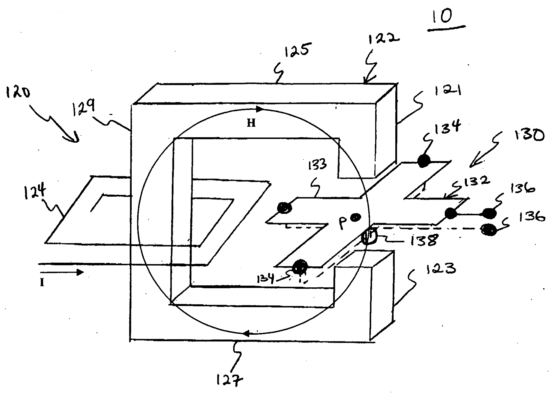
[0029]The present invention is directed to a magnetic memory device. In particular, FIG. 1 illustrates an exemplary embodiment of a memory cell of a magnetic memory device according to the present invention. A memory cell 10 according to an exemplary embodiment of the present invention includes a magnetic switch 120 and a sensor 130. The magnetic switch 120 includes a generally C-shaped magnetic component or material 122 and a coaxial coil 124 around one of the legs of the C-shaped magnetic component 122 to hold data. The sensor 130 includes a Hall effect sensor 132 and output terminals 136 connected to a voltage detector (not shown) to detect the stored data in the magnetic switch 120.

[0030]The C-shaped magnetic component 122 includes an upper leg 125, a lower leg 127, and a side leg 129. The upper and lower legs 125, 127 i...


PUM


Abstract

A non-volatile magnetic memory device having one or more memory cells, each of the memory cells includes a magnetic switch including a C-shaped magnetic component and a write coil located proximate the magnetic component, the write coil coupled to receive a current sufficient to create a remnant magnetic polarity in the magnetic component, and a Hall sensor, positioned proximate the magnetic component, to detect the remnant magnetic polarity indicative of a stored data bit.

Description

[0001]This application claims the benefit of pending U.S. provisional patent application No. 60 / 996,794, which was filed on Dec. 5, 2007 and is incorporated herein by reference in its entirety.FIELD OF THE INVENTION[0002]The present invention relates to a memory device and, more particularly, to a memory device using magnetic memory elements.BACKGROUND OF THE INVENTION[0003]The rapid growth in the portable consumer product market (including the products for portable computing and communications) is driving the need for low power consumption non-volatile memory devices, with their inherent ability to retain stored information without power. The principal technology currently available in the marketplace for these applications is EEPROM (Electrically Erasable Programmable Read-Only Memory) technology, relying on charging (writing) or discharging (erasing) the floating-gate of a Metal-Oxide-Semiconductor (N-type) type transistor using so-called Fowler-Nordheim tunneling through the ult...

Claims


Application Information

Patent Timeline
Patent Type & Authority Applications(United States)
IPC IPC(8): H01L29/82H01L21/00
CPCG11C11/18G01R33/07
Inventor KUPER, CYNTHIA A.IMAI, DARREN
Owner MICROMEM TECH
Why Eureka
Try Eureka