Method of making a semiconductor device with residual amine group free multilayer interconnection

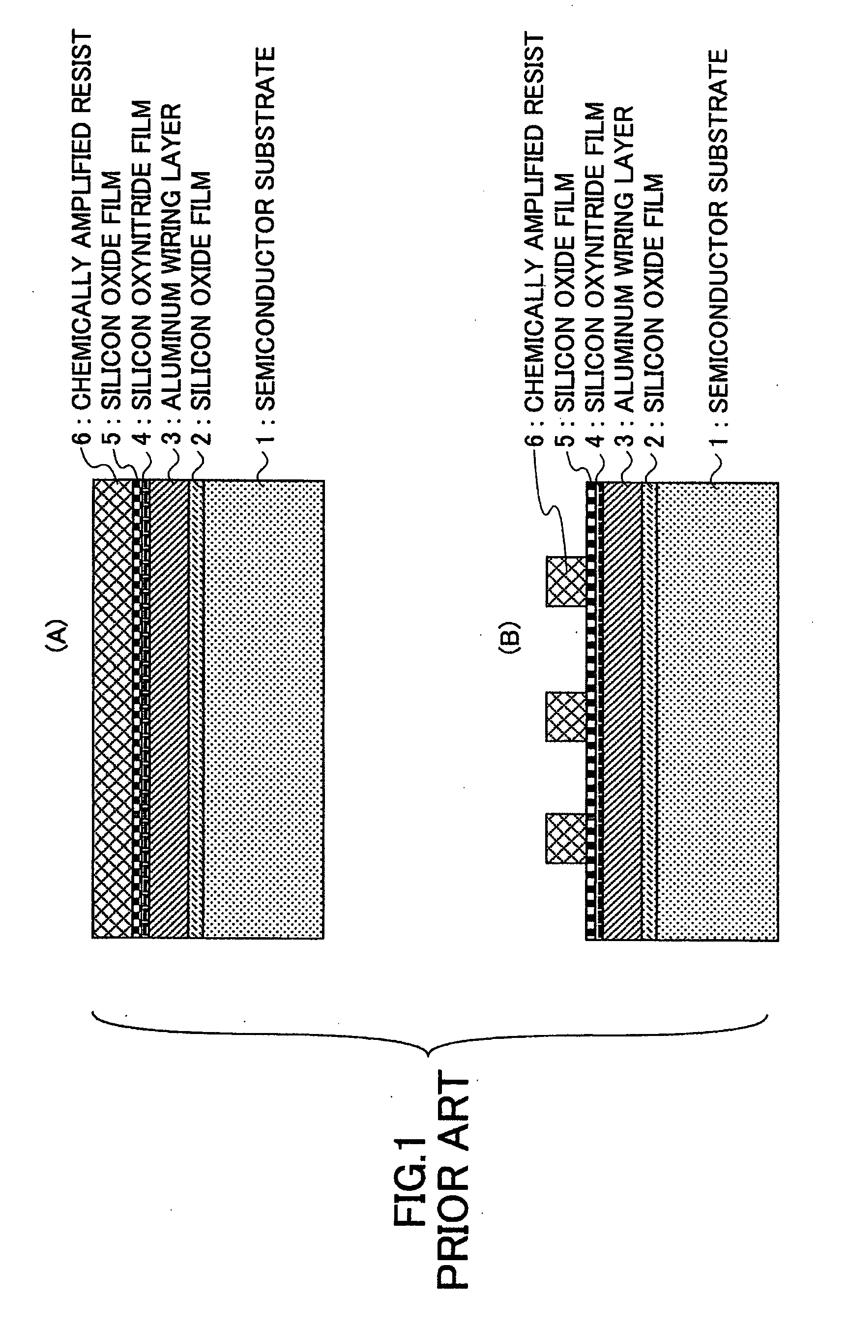
a multi-layer interconnection and semiconductor technology, applied in semiconductor/solid-state device details, photomechanical apparatus, semiconductor devices, etc., can solve the problems of preventing the oxidation reaction of the chemically amplified, unable to form a wiring pattern groove, and unstable silicon oxynitride film b>4/b>, etc., to achieve excellent patterning

Inactive Publication Date: 2009-06-11
FUJITSU MICROELECTRONICS LTD
View PDF17 Cites 3 Cited by
  • Summary
  • Abstract
  • Description
  • Claims
  • Application Information

AI Technical Summary

Benefits of technology

[0037]A more specific object of the present invention is to provide a semiconductor device that has a multilayered interconnection structure using a dual damascene process in which a silicon nitride film is formed as a reflection preventing film on a SiOC film as an interlayer insulating film. This semiconductor device prevents the dissolution hindering effect of the chemically amplified resist film, and has a high precision in patterning.
[0039]As the insulating film that does not contain nitrogen is formed between the interlayer insulating film made of a silicon oxide film containing carbon and the insulating film that contains nitrogen, the nitrogen gas generated during the formation of the insulating film containing nitrogen is prevented from diffusing into the interlayer insulating film made of a silicon oxide film containing carbon. Accordingly, the generation of an amine group such as NH due to the reaction of the nitrogen gas with the H group contained in the interlayer insulating film can be prevented. As a result, the dissolution hindering phenomenon in a chemically amplified resist film adjacent to the interlayer insulating film can be prevented, and excellent patterning can be performed for the semiconductor device having a multilayered interconnection structure.

Problems solved by technology

As the wavelength of the light source becomes shorter, however, the reflectivity of the substrate of the semiconductor device becomes higher, and the wavelength is restricted to a narrower band, often resulting in a standing wave.
With a standing wave, a defective pattern might be caused due to light leakage at the stepwise part of the semiconductor device, and the resolution line width is periodically varied with a change of the resist film thickness.
However, the silicon oxynitride film 4 is unstable as it is.
Such a neutralization reaction leads to problems of hindering an oxidation reaction of the chemically amplified resist film 6, and preventing the formation of a pattern on the chemically amplified resist film 6.
This leads to a problem of not being able to form a wiring pattern groove.
When the amine group reaches the chemically amplified resist film 231 in the via hole, the photooxide is neutralized, resulting in a hindrance to oxidation reaction.

Method used


Image

  • Method of making a semiconductor device with residual amine group free multilayer interconnection
  • Method of making a semiconductor device with residual amine group free multilayer interconnection
  • Method of making a semiconductor device with residual amine group free multilayer interconnection

Examples


first embodiment

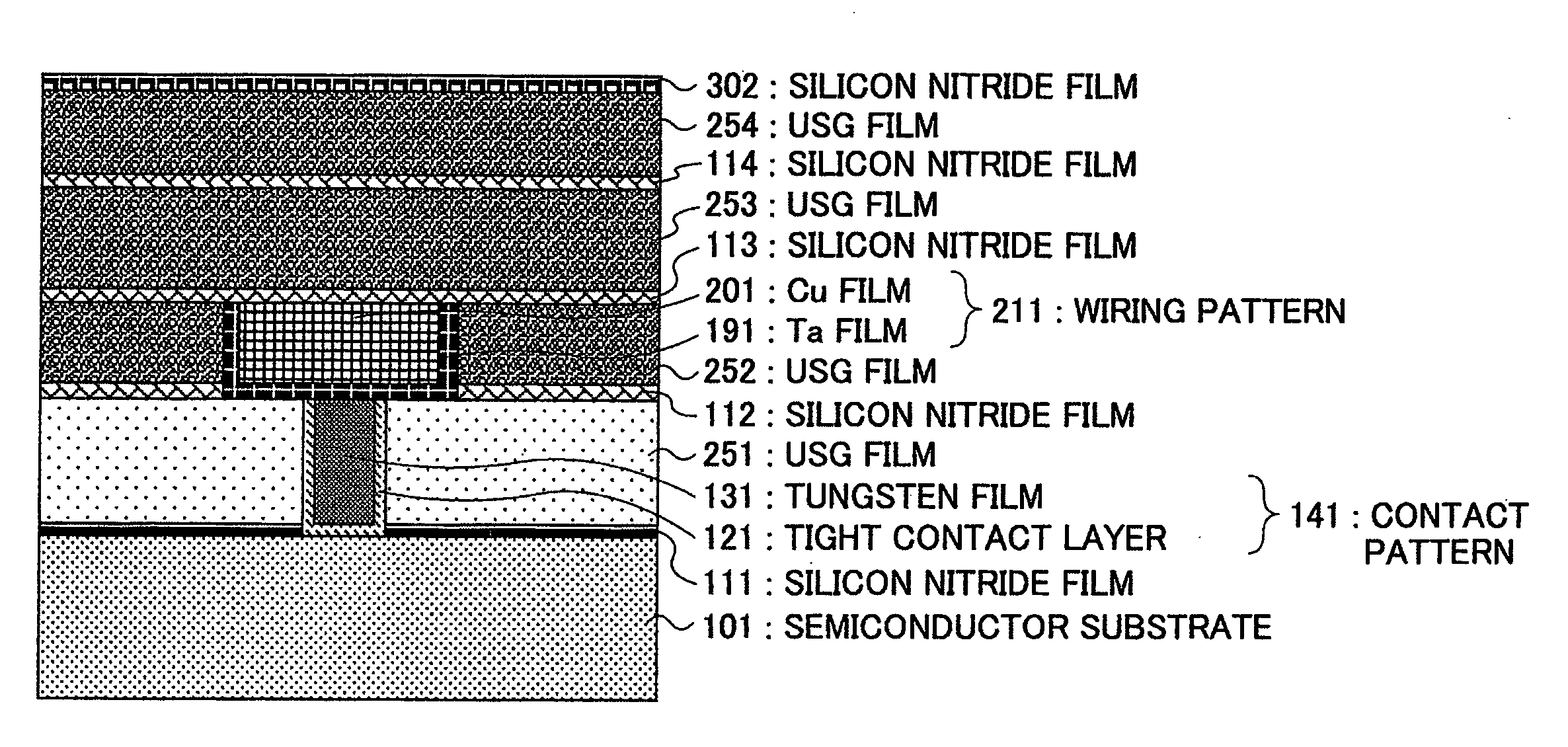
[0123]FIGS. 16 through 31 illustrate a process of manufacturing a semiconductor device in accordance with a first embodiment of the present invention. In this manufacturing process, a SiOC film that is an interlayer insulating film is patterned using a dual damascene process and a reflection preventing film.

Step of Forming a Contact Pattern

[0124]Referring to FIG. 16, after the formation of a circuit device (not shown) on a semiconductor substrate 101, a silicon nitride film 111 and a silicon oxide film 151 are formed on the semiconductor substrate 101. To flatten the area of the circuit device (not shown), the silicon oxide film 151 is polished by a CMP method. After that, a chemically amplifier resist film for forming a contact pattern (not shown) is patterned on the silicon oxide film 151. With the chemically amplified resist film being the mask, etching is performed to form a contact hole (not shown). A tight contact layer 121 and a tungsten film 131 are then formed in the contac...

second embodiment

[0143]Although the USG film 252 as a diffusion preventing film is formed between the SiOC film 163 and the silicon nitride film 302 as a reflection preventing film in the first embodiment of the method of manufacturing a semiconductor device, a SiC film not containing N as a growth gas may be employed instead of the USG film 252.

[0144]The growth gases for a SiC film include tetramethylsilane (Si(CH3)4) and CO2, as described earlier.

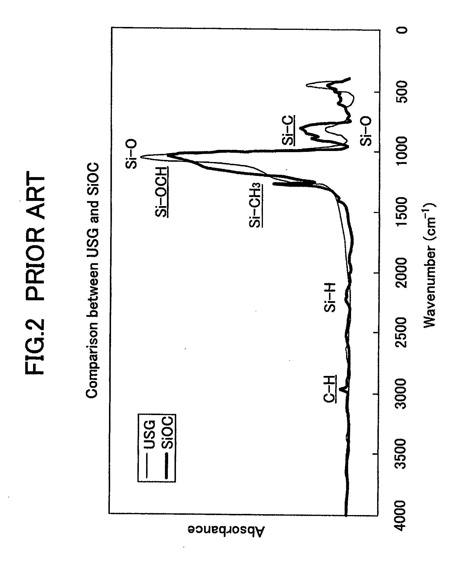
[0145]A SiC film as a diffusion preventing film is formed on the SiOC film 163, and the silicon nitride film 302 as a reflection preventing film is then formed on the SiC film. With this structure, the N2 gas generated during the formation of the silicon nitride film 302 as a reflection preventing film can be prevented from diffusing into the SiOC film 163 formed under the silicon nitride film 302 as a reflection preventing film. Also, the N2 gas can be prevented from reacting with the H group contained in the SiOC film 163, and generation of an amine gro...

third embodiment

[0146]Although the USG film 252 as a diffusion preventing film is formed between the SiOC film 163 and the silicon nitride film 302 as a reflection preventing film in the first embodiment of the method of manufacturing a semiconductor device, a PSG film not containing N as a growth gas may be employed instead of the USG film 252.

[0147]The growth gases for a PSG film include PH3, O2, and He.

[0148]More specifically, a PSG film as a diffusion preventing film is formed on the SiOC film 163, and the silicon nitride film 302 as a reflection preventing film is then formed on the PSG film. With this structure, the N2 gas generated during the formation of the silicon nitride film 302 as a reflection preventing film can be prevented from diffusing into the SiOC film 163 formed under the SiN film 302. Also, the N2 gas can be prevented from reacting with the H group in the SiOC film 163, and generation of an amine group such as NH in the SiOC film 163 can be prevented. Thus, the dissolution hin...


PUM

PropertyMeasurementUnit
thicknessaaaaaaaaaa
thicknessaaaaaaaaaa
wavelengthaaaaaaaaaa

Abstract

The present invention provides a semiconductor device that can restrict the dissolution hindering phenomenon in a chemically amplified resist film. More specifically, after the formation of a contact pattern on a semiconductor substrate, a wiring pattern is formed on the contact pattern. A SiC film, a first SiOC film, a SiC film, a second SiOC film, a USG film as a diffusion preventing film, and a silicon nitride film as a reflection preventing film, are formed on the wiring pattern. A dual damascene structure is then formed using the chemically amplified resist film and another chemically amplified resist film. In this manner, the N2 gas generated during the formation of the silicon nitride film as a reflection preventing film can be prevented from diffusing into the second SiOC film formed under the silicon nitride film. Accordingly, the reaction of the N2 gas with the H group contained in the second SiOC film and the generation of an amine group such as NH in the second SiOC film can be prevented. Thus, the dissolution hindering phenomenon in the chemically amplified resist film can be avoided.

Description

INCORPORATION-BY-REFERENCE TO RELATED APPLICATIONS[0001]This application is a divisional application of Ser. No. 10 / 385,729, filed Mar. 12, 2003, and is based upon and claims the benefit of priority from the prior Japanese Patent Application No. 2002-166897, filed in Jun. 7, 2002, the entire contents of which are incorporated by reference.BACKGROUND OF THE INVENTION[0002]The present invention generally relates to semiconductor devices, and, more particularly, to a semiconductor device that is formed with an oxide film containing C or H as an interlayer insulating film and a chemically amplified photoresist.[0003]There has been an increasing demand for smaller semiconductor devices that consume less electricity and yet are capable of performing higher-speed operations. To satisfy such a demand, a Cu-damascene process using Cu with a lower resistivity is employed to form wiring structures, especially, multilayered interconnection structures. At the same time, employment of low-dielect...

Claims


Application Information

Patent Timeline
Patent Type & Authority Applications(United States)
IPC IPC(8): H01L21/31H01L21/02G03F7/11H01L21/027H01L21/311H01L21/316H01L21/318H01L21/768H01L23/522H01L23/532
CPCH01L21/31144H01L21/31612H01L21/3185H01L21/76808H01L23/53238H01L2924/0002H01L23/5329H01L23/53295H01L2924/00H01L21/02126H01L21/02167H01L21/02129H01L21/02203H01L21/022H01L21/3205
Inventor KAKAMU, KATSUMIWATATANI, HIROFUMIIKEDA, MASANOBU
Owner FUJITSU MICROELECTRONICS LTD
Why Eureka
Try Eureka