

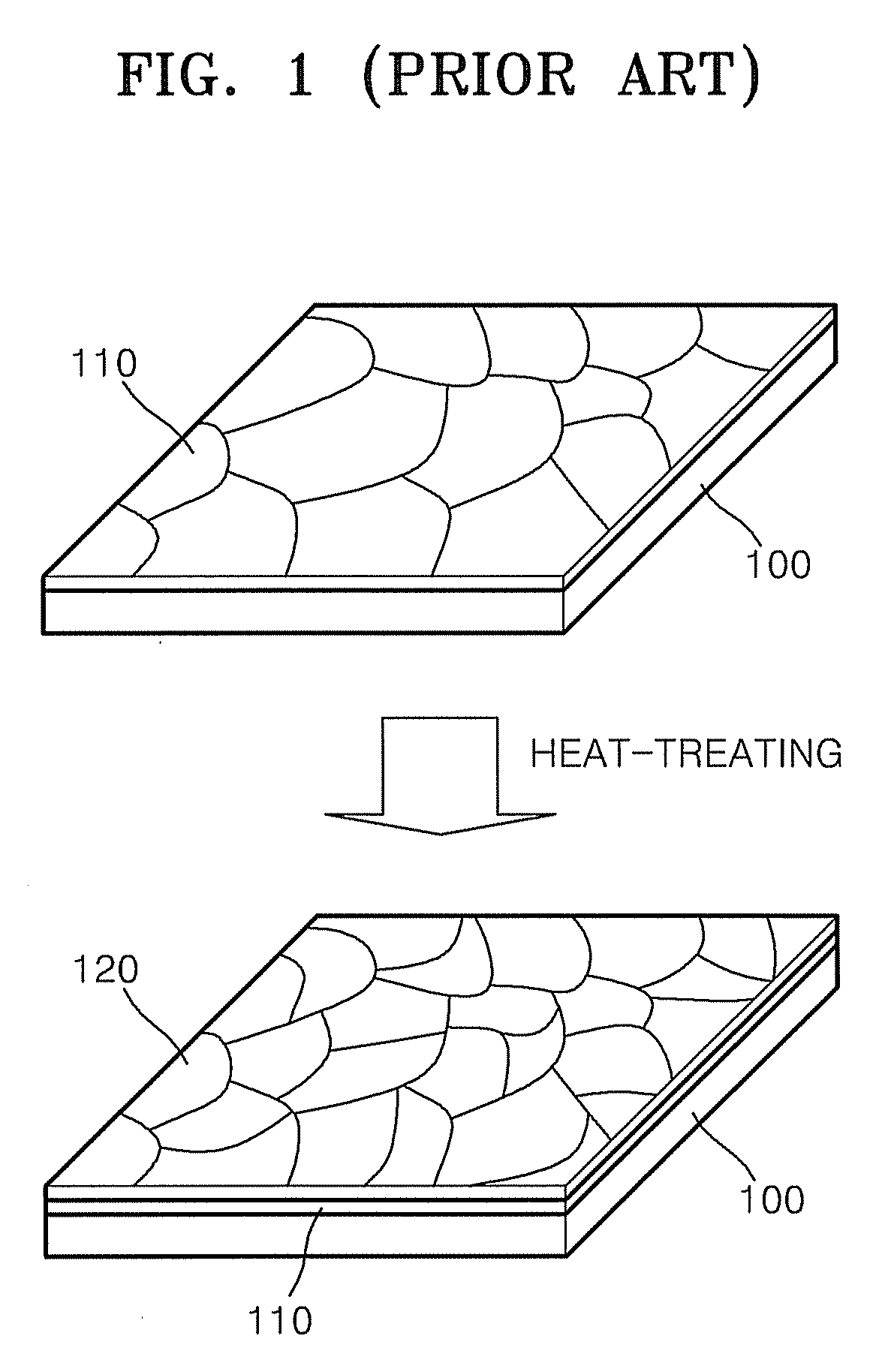
Single crystalline graphene sheet and process of preparing the same
a single crystal, graphene sheet technology, applied in the direction of polycrystalline material growth, gel state, synthetic resin layered products, etc., can solve the problems of high cost of carbon nanotubes, difficulty in separating single-walled carbon nanotubes, and inability to include a uniform number of layers in the separated graphene sh
- Summary
- Abstract
- Description
- Claims
- Application Information
AI Technical Summary
Benefits of technology
Problems solved by technology
Method used
Image

Examples
example 1
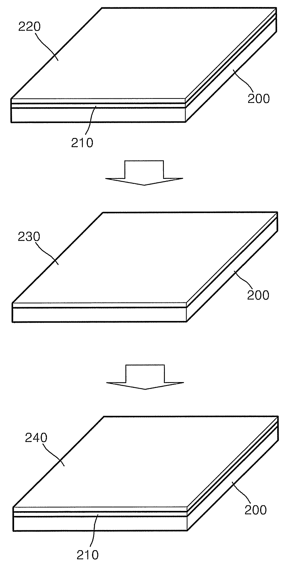
[0089]A single-crystal Ni thin film having a diameter of 1.2 cm and a thickness of 0.2 mm (having a (111) surface, Matec, Inc.) was placed in a reaction chamber, and heat-treated at 700° C. for 1 hour while flowing hydrogen into the chamber at 60 sccm to remove an oxide formed on the surface of the single-crystal Ni thin film. Then, the single crystal Ni thin film was heat-treated at 750° C. for 2 minutes using a halogen lamp heat source while introducing acetylene gas and hydrogen gas into the chamber at 5 sccm and 45 sccm respectively to form graphene on the single-crystal Ni thin film graphitizing catalyst.
[0090]Then, the heat source was removed and the chamber was naturally cooled to grow the graphene to a constant thickness, thereby forming a graphene sheet having a diameter of 1.2 cm and about 7 layers.
[0091]Then, the single-crystal Ni thin film on which the graphene sheet formed was dissolved by treatment in 0.1 M HCl for 24 hours to remove the Ni thin film and yield the sing...
example 2
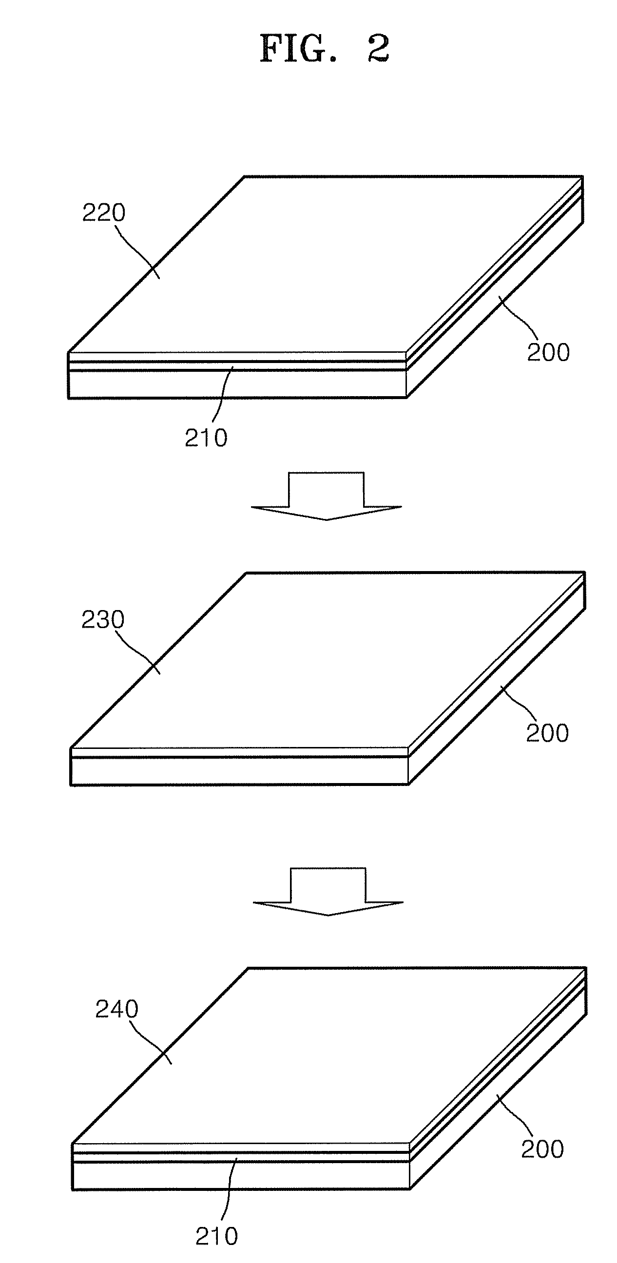
[0093]A Ni single crystal having a diameter of 1.2 cm and a thickness of 0.2 mm (having a (111) surface, Matec, Inc.) was placed in a reaction chamber on a _ substrate, and heat-treated at 700° C. for 1 hour while flowing hydrogen into the chamber at 60 sccm to remove an oxide formed on the surface of the single crystalline Ni. Then, the Ni single-crystal was heat-treated at 900° C. for 2 minutes using a halogen lamp heat source while introducing acetylene gas and hydrogen gas into the chamber at 5 sccm and 45 sccm respectively to form graphene.
[0094]Then, the heat source was removed and the chamber was naturally cooled to grow the graphene to a constant thickness, thereby forming a graphene sheet having a diameter of 1.2 cm and about 7 layers.
[0095]Then, the substrate on which the graphene sheet is formed was dissolved by treatment in 0.1 M HCl for 24 hours to remove the Ni thin film and yield the single-crystal graphene sheet.
[0096]FIG. 6 is a graph illustrating a Raman spectrum o...
PUM
| Property | Measurement | Unit |
|---|---|---|
| length | aaaaa | aaaaa |
| temperature | aaaaa | aaaaa |
| temperature | aaaaa | aaaaa |
Abstract
Description
Claims
Application Information