Electroluminescent Devices

Inactive Publication Date: 2009-07-02
MERCK PATENT GMBH
View PDF7 Cites 30 Cited by
  • Summary
  • Abstract
  • Description
  • Claims
  • Application Information

AI Technical Summary

Benefits of technology

[0010]We have now devised an electroluminescent device with an intermediate light absorbing layer which reduces this problem.
[0018]There can optionally be layers of other compounds e.g. LiF which improve the functioning of the device such as buffer layers.

Problems solved by technology

However, these suffer from the disadvantages of high energy consumption, high cost of manufacture, low quantum efficiency and the inability to make flat panel displays.
However the materials used as an intermediate light absorbing layer can adversely affect the performance of the electroluminescent material.
For example, the known and used reflectivity influencing materials are deposited by sputtering which adversely affects the performance of the EL device.
An alternative method is to form the cathode so that it is thin enough to be partially or substantially transmissive to light and to have a light absorbing layer behind the cathode; however this type of structure adversely affects the choice and nature of the cathode which can be used.

Method used


Image

  • Electroluminescent Devices
  • Electroluminescent Devices
  • Electroluminescent Devices

Examples


example 4

PREPARATIVE EXAMPLE 4
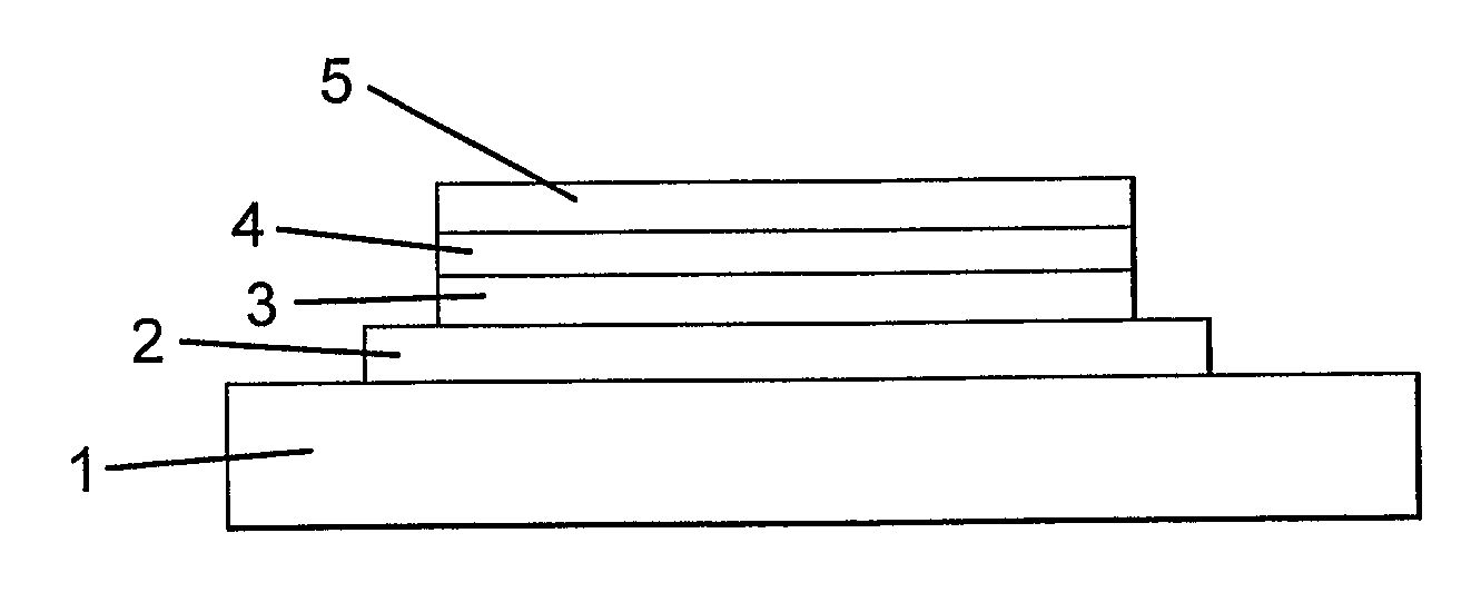
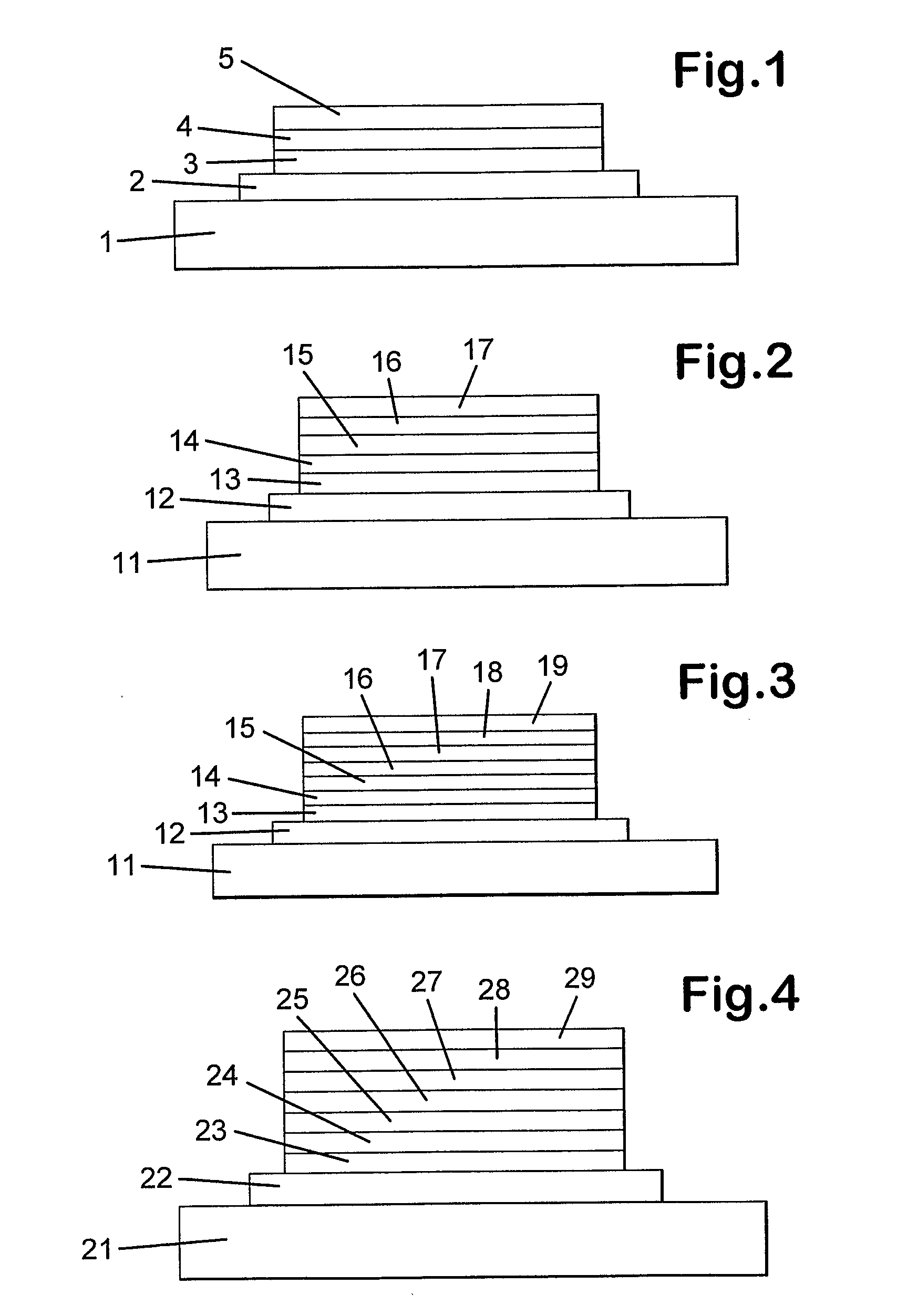
Device Structure

[0126]A pre-etched ITO coated glass piece (10×10 cm2) was used. The device was fabricated by sequentially forming layers on the ITO, by vacuum evaporation using a Solciet Machine, ULVAC Ltd. Chigacki, Japan. The active area of each pixel was 3 mm by 3 mm. The coated electrodes were encapsulated in an inert atmosphere (nitrogen) with V-curable adhesive using a glass back plate. Electroluminescence studies were performed with the ITO electrode was always connected to the positive terminal. The current vs. voltage studies were carried out on a computer controlled Keithly 2400 source meter.

example 1

[0127]Devices were formed by the method described above consisting of:

ITO / ZnTP TP (20) / α-NBP(75) / AlQ3.DPQA (75:0.2) / ZrQ4 (20) / KL(x) / LiF(0.3) / Al

ITO / ZnTP TP (20) / KL(x) / α-NBP(75) / AlQ3.DPQA (75:0.2) / ZrQ4(20) / LiF(0.3) / Al

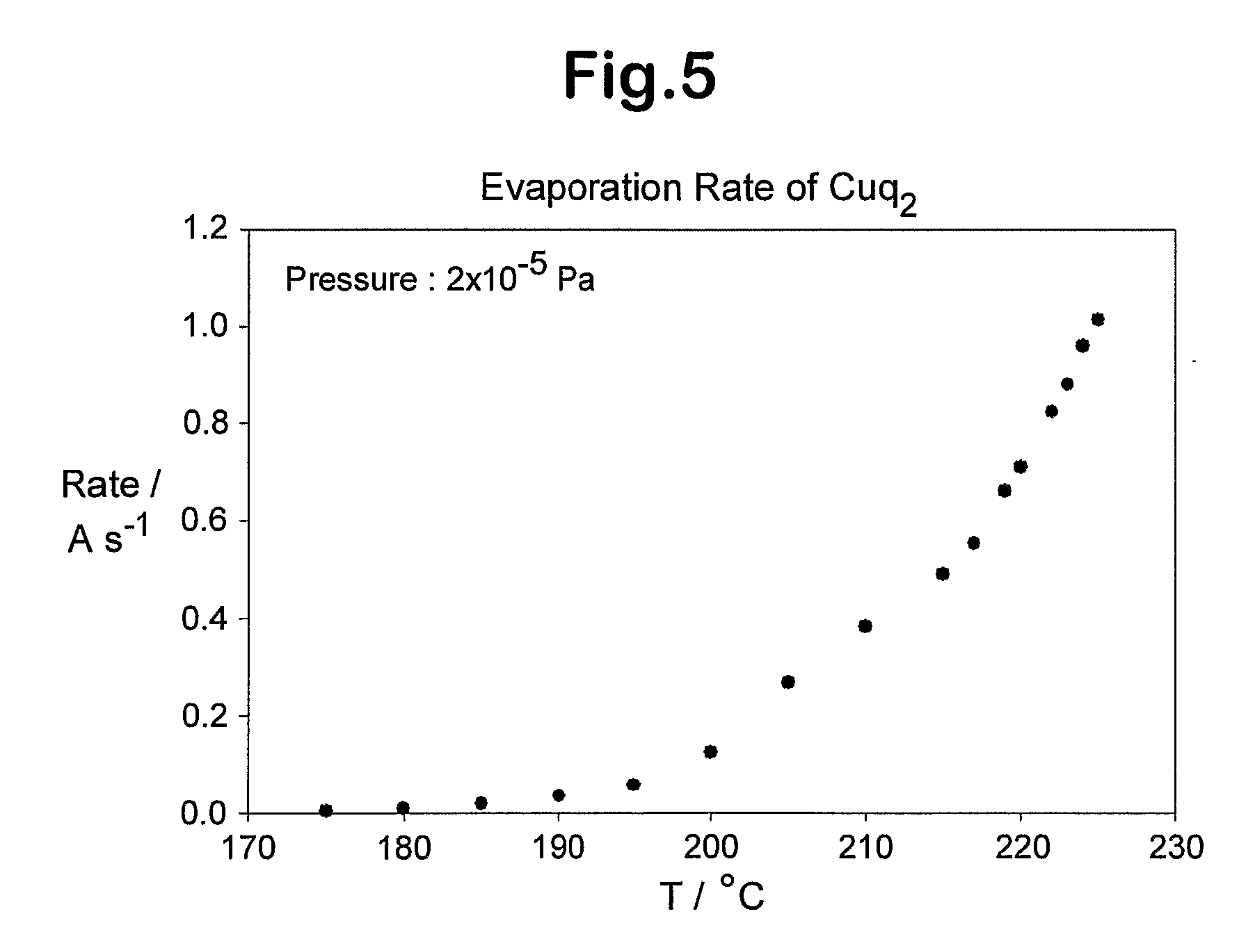
[0128]wherein ZnTP TP represents zinc phthalocyanine of formula indicated below, α-NBP has the structure indicated below, and KL(X) indicates CuQ2 in the thickness in nm indicated. The performance of the devices was measured and the results are as shown in FIGS. 5-21. A spectrum of a similar cell without CuQ2 is shown at FIG. 22. Note in relation to the thicknesses of the LiF that the quoted value is sometimes 0.3 nm and sometimes 0.5 nm, no significance flowing from that difference which is within experimental error.

example 2

[0129]Devices were formed by the method described above consisting of:

ITO / ZnTP TP (20) / α-NBP(75) / AlQ3.DPQA (75:0.2) / Zrq4 (20) / KL(x) / LiF(0.3) / Al

[0130]in which in this instance KL(x) represents VOq2. The performance of the devices was measured and the results are as shown in FIGS. 23-24.


PUM


Abstract

In an OLED there is a reflectivity influencing layer (27) which is preferably semi-absorbent and in embodiments is dark coloured or black which is formed of a sublimable organometallic compound. The reflectivity influencing layer is formed between an electrode (29 or 22) and a light-emitting layer (25).

Description

FIELD OF THE INVENTION[0001]This invention relates to electroluminescent devices which may be based on inorganic, polymeric, metal complex or organometallic electroluminescent materials and have a contrast enhancing layer.BACKGROUND TO THE INVENTION[0002]Except where otherwise indicated, the disclosures of all documents mentioned herein are incorporated herein by reference.[0003]Materials which emit light when an electric current is passed through them are well known and used in a wide range of display applications. Liquid crystal devices and devices which are based on inorganic semiconductor systems are widely used. However, these suffer from the disadvantages of high energy consumption, high cost of manufacture, low quantum efficiency and the inability to make flat panel displays.[0004]In one type of electroluminescent device there are successive layers comprising a transparent first electrode e.g. formed of an indium tin oxide coated glass which is the anode, optionally a hole tr...

Claims


Application Information

Patent Timeline
IPC IPC(8): H01L51/54H01L51/00H01L51/50H01L51/52
CPCC09K11/06C09K2211/188H01L51/006H01L51/0077H05B33/14H01L51/5036H01L51/5092H01L51/5284H01L51/0078H10K85/633H10K85/311H10K85/30H10K50/125H10K50/171H10K50/865
Inventor KATHIRGAMANATHAN, POOPATHYRAVICHANDRAN, SEENIVASAGAMCHAN, YUN FU
Owner MERCK PATENT GMBH
Why Eureka
Try Eureka