Voltage controlled ring oscillator
a voltage control and ring oscillator technology, applied in the direction of oscillator generators, pulse generation by logic circuits, pulse techniques, etc., can solve the problems of voltage scaling, deterioration of the performance of the pll (phase locked loop) circuit, and very high gain of the vco at the characteristic typ
- Summary
- Abstract
- Description
- Claims
- Application Information
AI Technical Summary
Benefits of technology
Problems solved by technology
Method used
Image
Examples
first embodiment
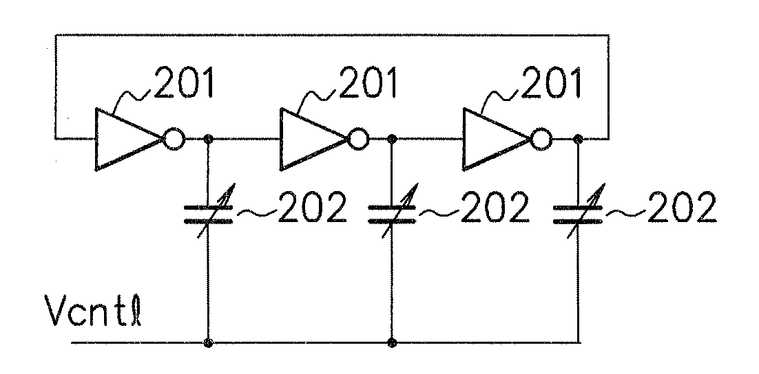
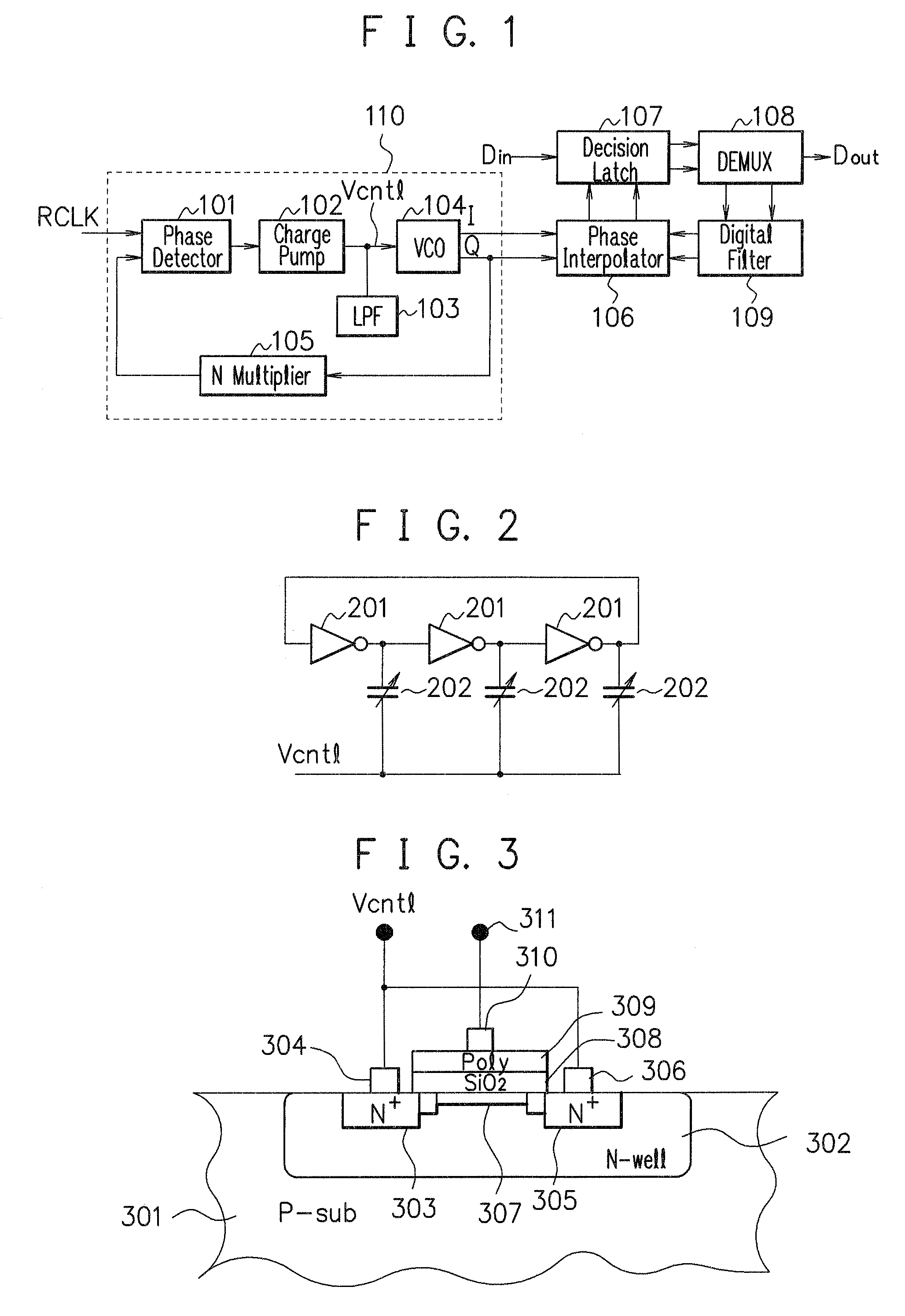
[0050]FIG. 1 is a view showing a structural example of a high speed input / output (I / O) circuit according to the present invention. In case of the high speed I / O circuit, a frequency clock being half of the data rate is required from a driver (Tx) and a receiver (Rx), in which the clock is generated by a PLL circuit 110. The PLL circuit 110 has a phase detector 101, a charge pump 102, a loop filter (LPF) 103, a voltage controlled oscillator (VCO) 104, and a multiplier 105. The phase detector 101 compares a reference clock RCLK with an output clock (feedback clock) output from the multiplier 105, and then outputs a pulse width corresponding to the phase error to the charge pump 102. The charge pump 102 flows a current corresponding to the pulse width through the LPF 103. The LPF 103 is a low-pass filter which smoothes the error signal. The VCO 104 oscillates in accordance with the smoothed voltage Vcntl, and outputs I signals and Q signals. For instance, the I signals are differential...
second embodiment
[0064]FIG. 8A is a block diagram showing a structural example of a PLL circuit according to the present invention. The PLL circuit is the same as the PLL circuit 110 in FIG. 1.
[0065]FIG. 8B is a circuit diagram showing a structural example of a VCO 104 in FIG. 8A. The VCO 104 is the same as the VCO in FIG. 4.
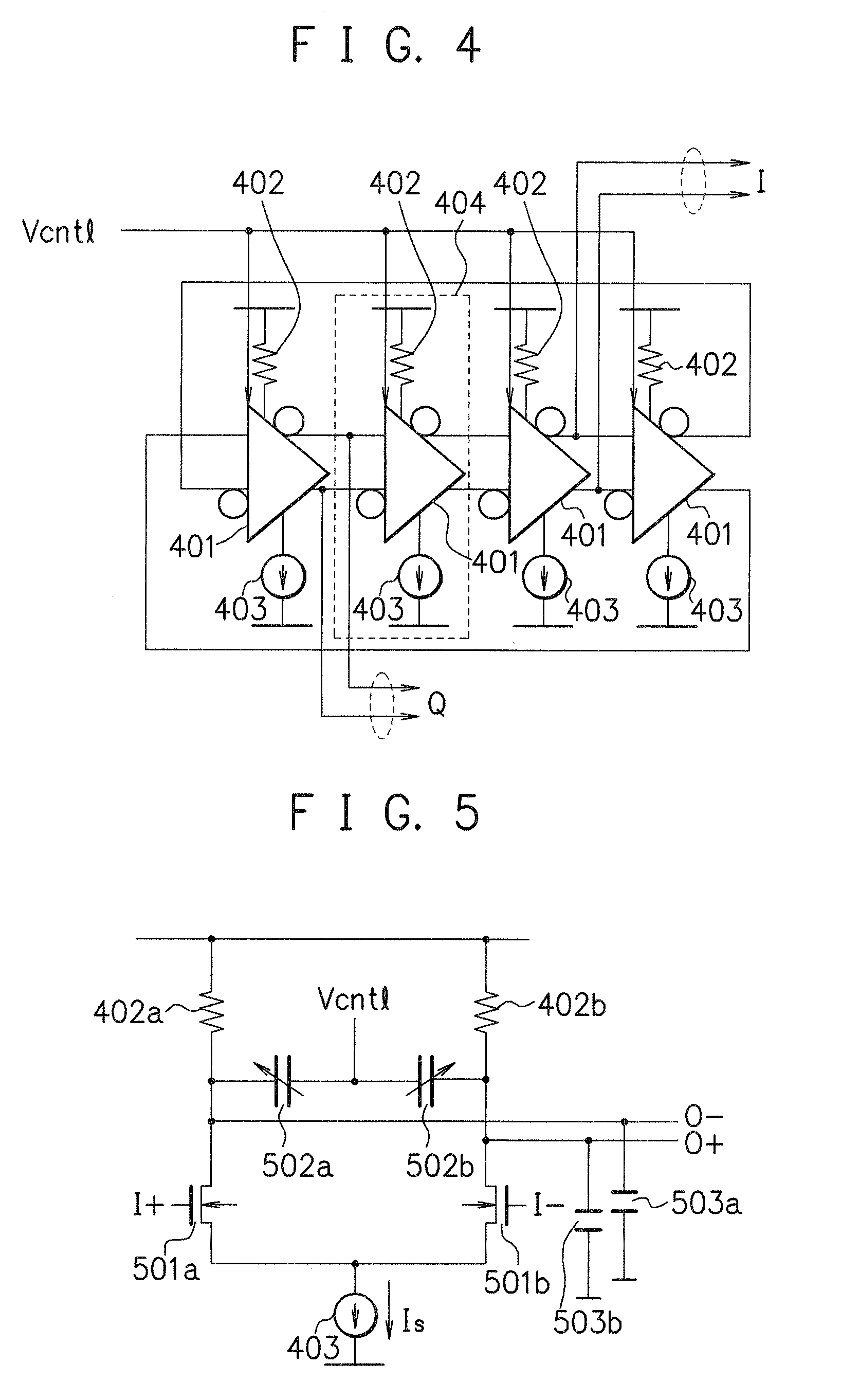
[0066]FIG. 8C is a circuit diagram showing a structural example of a CR ring element 404 in FIG. 8B. A point where the present embodiment is different from FIG. 5 will be explained. An N-channel transistor 801 corresponds to the current source 403 in FIG. 5, and having a gate, a source, and a drain respectively connected to a fixed voltage Vb, a ground, and an interconnection point of sources of the transistors 501a and 501b. The CR ring element 404 is a CR delay element in which resistors (R) 402a and 402b are fixed and capacitances (C) 502a and 502b are variable. The CR ring element 404 has a CML-type differential amplifier, and applies pure resistors 402a and 402b as loads in...
third embodiment
[0068]FIG. 9A is a block diagram showing a structural example of a PLL circuit according to the present invention. The PLL circuit is the same as the PLL circuit in FIG. 8A.
[0069]FIG. 9B is a circuit diagram showing a structural example of a VCO 104 in FIG. 9A. The VCO 104 is the same as the VCO in FIG. 8B.
[0070]FIG. 9C is a circuit diagram showing a structural example of a CR ring element 404 in FIG. 9B. A point where the present embodiment is different from FIG. 8C will be explained. Load resistor units 901a and 901b are provided in place of the load resistors 402a and 402b in FIG. 8C.
[0071]FIG. 9D is a view showing a structural example of the respective load resistor units 901a and 901b in FIG. 9C. The load resistor units 901a and 901b are composed of P-channel transistors 902. The transistor 902 is connected at a gate thereof to a fixed voltage Vb1, at a source thereof to the power supply voltage, and at a drain thereof to a drain of either the transistor 501a or the transistor ...
PUM
 Abstract
Description
Claims
Application Information


