Contact for a semiconductor light emitting device

a light-emitting device and semiconductor technology, applied in the field of ##light-emitting diodes, can solve the problems the use of thick semiconductor layers has several disadvantages, etc., and achieves the effect of reducing reducing the contact resistance, and improving the reflectivity of the conta

Inactive Publication Date: 2009-07-09
LUMILEDS
View PDF15 Cites 22 Cited by
  • Summary
  • Abstract
  • Description
  • Claims
  • Application Information

AI Technical Summary

Benefits of technology

[0006]In order to minimize the contact resistance on the p-side of the light emitting layer, the semiconductor structure may include a p-type contact layer disposed between the p-type region and the p-contact. The interface between the p-type contact layer and the p-contact may be configured such that when the device is forward biased, carriers tunnel through the interface. As a result, the contact need not be annealed, which may improve the reflectivity of the contact, as annealing generally causes alloying between the semiconductor material and the metal contact which often reduces the reflectivity of the contact. In some embodiments, the p-contact layer is one of GaP, AlGaInP, and InGaP, doped at least in portions to a hole concentration of at least 5×1018 cm−3. The p-contact may be a full sheet of metal, which increases the optical reflectivity, minimizes the electrical contact resistance and decreases the thermal impedance of the device. A tunneling contact may permit the use of a variety of highly reflective metals for the p-contact, such as Ag.

Problems solved by technology

The use of thick semiconductor layers has several disadvantages over other approaches, however, due to the tradeoff between light absorption and electrical and thermal resistivity common in semiconductor materials.
As a result, the contact need not be annealed, which may improve the reflectivity of the contact, as annealing generally causes alloying between the semiconductor material and the metal contact which often reduces the reflectivity of the contact.

Method used


Image

  • Contact for a semiconductor light emitting device
  • Contact for a semiconductor light emitting device
  • Contact for a semiconductor light emitting device

Examples


Embodiment Construction

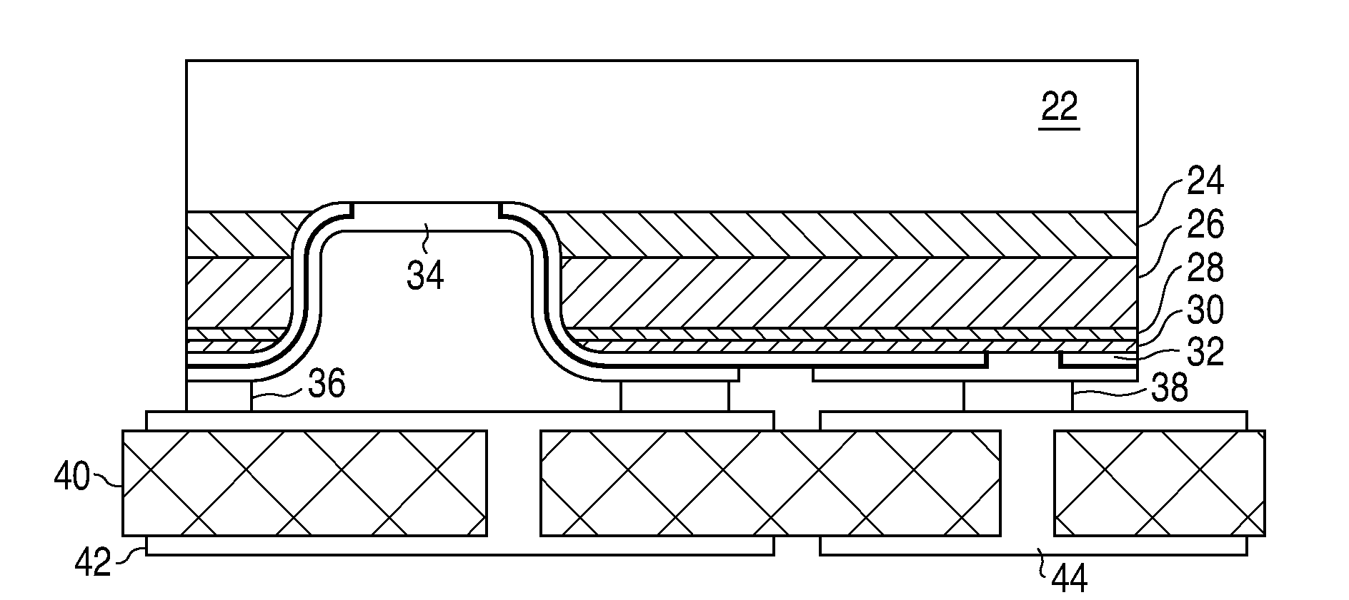
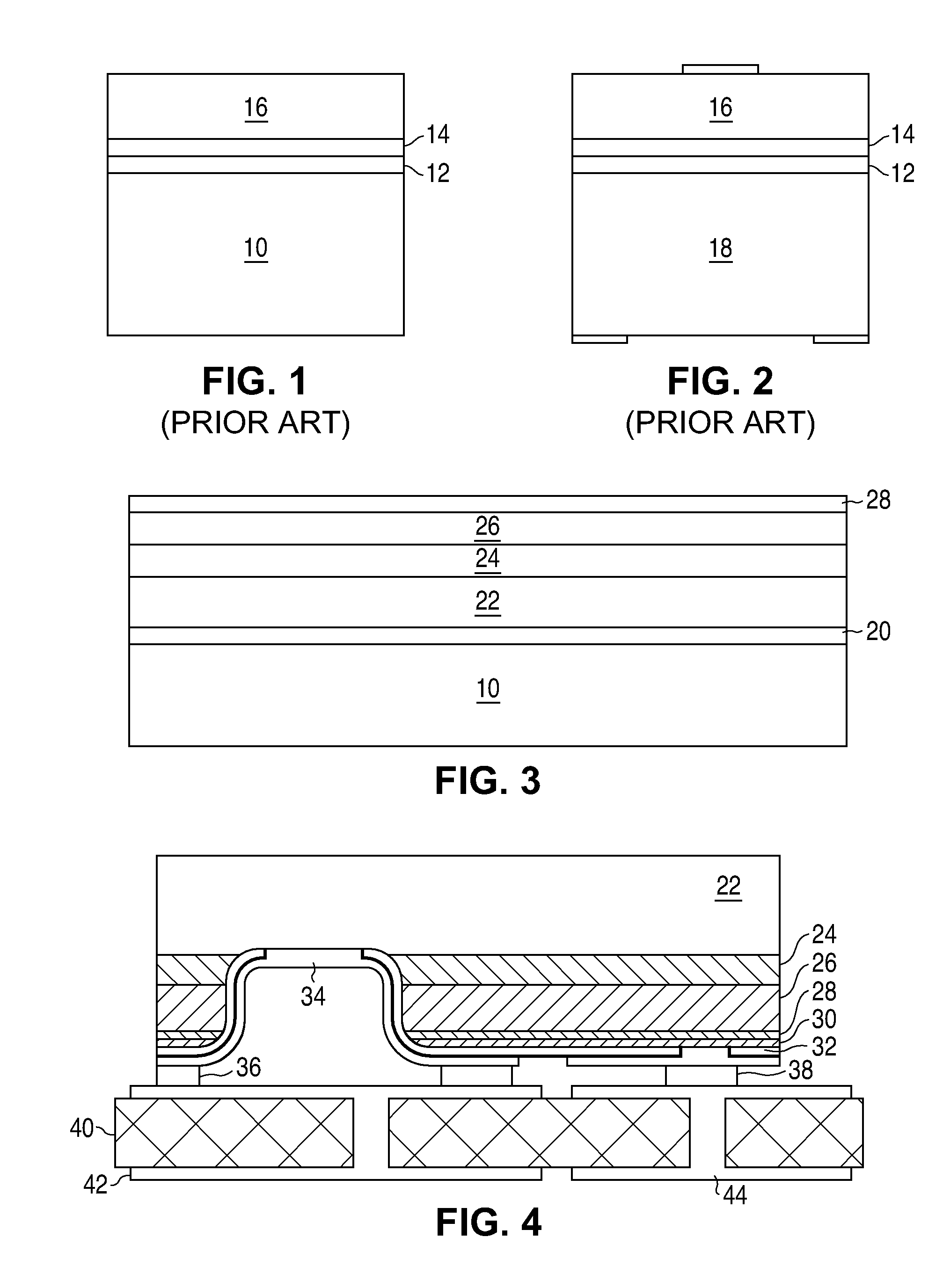
[0014]Depending on the context, as used herein, “AlGaInP” may refer in particular to a quaternary alloy of aluminum, indium, gallium, and phosphorus, or in general to any binary, ternary, or quaternary alloy of aluminum, indium, gallium, and phosphorus. Depending on the context, as used herein, “contact” may refer in particular to a metal electrode, or in general to the combination of a semiconductor contact layer, a metal electrode, and any structures disposed between the semiconductor contact layer and the metal electrode.

[0015]As described above, AlGaInP devices have conventionally included thick layers, particularly on the p-side of the light emitting region, for current spreading, due to the low mobility of holes in p-type AlGaInP material. Thinner p-type layers have generally not been used due to the difficulty of achieving high hole concentrations in AlGaInP.

[0016]In accordance with embodiments of the invention, an AlGaInP light emitting device includes a highly doped, thin p...


PUM


Abstract

An AlGaInP light emitting device is formed as a thin, flip chip device. The device includes a semiconductor structure comprising an AlGaInP light emitting layer disposed between an n-type region and a p-type region. N- and p-contacts electrically connected to the n- and p-type regions are both formed on the same side of the semiconductor structure. The semiconductor structure is connected to the mount via the contacts. The growth substrate is removed from the semiconductor structure and the thick transparent substrate is omitted, such that the total thickness of semiconductor layers in the device is less than 15 μm in some embodiments, less than 10 μm in some embodiments. The top side of the semiconductor structure may be textured.

Description

BACKGROUNDDescription of Related Art[0001]Light emitting diodes (LEDs) are widely accepted as light sources in many applications that require low power consumption, small size, and high reliability. Energy-efficient diodes that emit light in the yellow-green to red regions of the visible spectrum contain active layers formed of an AlGaInP alloy. FIGS. 1 and 2 show the fabrication of a conventional transparent substrate (TS) AlGaInP LED. In FIG. 1, an etch stop layer 12, such as a 1000 Å n-In0.5Ga0.5P layer, is grown over a semiconductor substrate 10, typically GaAs. Device layers 14, including a lower confining layer, at least one (AlxGal1-x)yIn1-yP active layer, and an upper confining layer, all placed in a double heterostructure configuration, are grown over etch stop layer 12, followed by an optional thick (for example, between 5 and 100 μm thick) window layer 16, often p-type GaP grown by vapor phase epitaxy. The confining layers are made of a transparent semiconductor and enhan...

Claims


Application Information

Patent Timeline
Patent Type & Authority Applications(United States)
IPC IPC(8): H01L33/00H01L21/02H01L33/40H01L33/48
CPCH01L33/0079H01L33/405H01L33/486H01L2924/0002H01L2924/00H01L33/0093
Inventor ALDAZ, RAFAEL I.EPLER, JOHN E.GRILLOT, PATRICK N.KRAMES, MICHAEL R.
Owner LUMILEDS
Why Eureka
Try Eureka