Polycrystalline silicon solar cell having high efficiency and method for fabricating the same

a solar cell and polycrystalline silicon technology, applied in the field of polycrystalline silicon solar cells, can solve the problems of low efficiency, reduced production cost, and inability to manufacture solar cells having a thickness of 300 m or less, and achieve the effect of high efficiency

Active Publication Date: 2009-07-16
SEOUL NAT UNIV R&DB FOUND
View PDF3 Cites 26 Cited by
  • Summary
  • Abstract
  • Description
  • Claims
  • Application Information

AI Technical Summary

Benefits of technology

[0028]Accordingly, the present invention has been made keeping in mind the above problems occurring in the prior art, and an object of the present invention is to provide a method of fabricating a high efficiency polycrystalline silicon solar cell, in which a light-absorbing layer is formed of non-polluted polycrystalline silicon using a metal-induced lateral crystallization (MILC) method, and grains of the polycrystalline silicon are vertically grown in the direction in which electrons and holes move using a metal induced vertical crystallization (MIVC) method in which the polycrystalline silicon is used as a crystallization seed, with the result that grain boundaries, acting as sites in which electrons and holes are recombined with each other, is minimized, thereby increasing the efficiency of a solar cell.

Problems solved by technology

However, when an ingot is cut into a silicon wafer, it is difficult to cut it to have a thickness of 300 μm or less, and the silicon wafer can be damaged in subsequent processes, so that it is impossible to manufacture a solar cell having a thickness of 300 μm or less.
In this technology of manufacturing the a-Si thin film solar cell, its production cost can be decreased by reducing the thickness of the silicon constituting the a-Si thin film solar cell, but the a-Si thin film solar cell manufactured using this technology has basic problems in that its efficiency is lower than that of the single-crystalline silicon (c-Si) solar cell and in that its properties are deteriorated by the Staebler-Wronski' effect when it is exposed to light for a long period of time.
The basic problems have not been completely solved yet although 20 years have passed since then.
It is analyzed that the reason why this a-Si thin film solar cell has low efficiency and stability is that its silicon thin film, which is a light-absorbing layer, is amorphous.
However, in the case of the PECVD system, it is known that a process of forming a silicon thin film is excessively sensitive to the temperature of a substrate, and the silicon thin film formed using this PECVD system is very porous.
Further, in the case of the HWCVD system, it is difficult to apply the HWCVD system to a large area system, this HWCVD system cannot be easily used to manufacture a solar cell.
Among them, the method of crystallizing amorphous silicon using a laser is not suitable for a process of manufacturing a solar cell, the process necessarily requiring a large area, because high-priced equipment is used.
When this MIC is directly used to manufacture a solar cell, a large-sized polycrystalline silicon thin film can be formed, but the efficiency of a solar cell is decreased due to the contamination of metals included in the polycrystalline silicon, and thus it is difficult to manufacture a high-efficiency solar cell.
Since sequential lateral crystallization (SLC) using a laser is used in this technology, problems related to the recombination of holes and electrons due to catalytic metals do not occur, but this technology is problematic in that large-area amorphous silicon cannot be efficiently crystallized and in that productivity is low compared to crystallization heat treatment using a furnace.
When the light-absorbing layer 3 is formed by crystallizing amorphous silicon into polycrystalline silicon using a conventional crystallization method, as shown in FIG. 2, grains 3b are randomly grown, so that a plurality of grain boundaries 3a, acting as the recombination sites of electrons ({circle around (e)}−) and holes ({circle around (h)}+) generated from the light-absorbing layer 3, is formed, with the result that there is a problem in that the efficiency of a solar cell is decreased.

Method used


Image

  • Polycrystalline silicon solar cell having high efficiency and method for fabricating the same
  • Polycrystalline silicon solar cell having high efficiency and method for fabricating the same
  • Polycrystalline silicon solar cell having high efficiency and method for fabricating the same

Examples


Embodiment Construction

[0047]Various objects, advantages and features of the invention will become apparent from the following description of embodiments with reference to the accompanying drawings.

[0048]Hereinafter, a preferred embodiment of the present invention will be described in detail with reference to the attached drawings.

[0049]Reference now should be made to the drawings, in which the same reference numerals are used throughout the different drawings to designate the same or similar components.

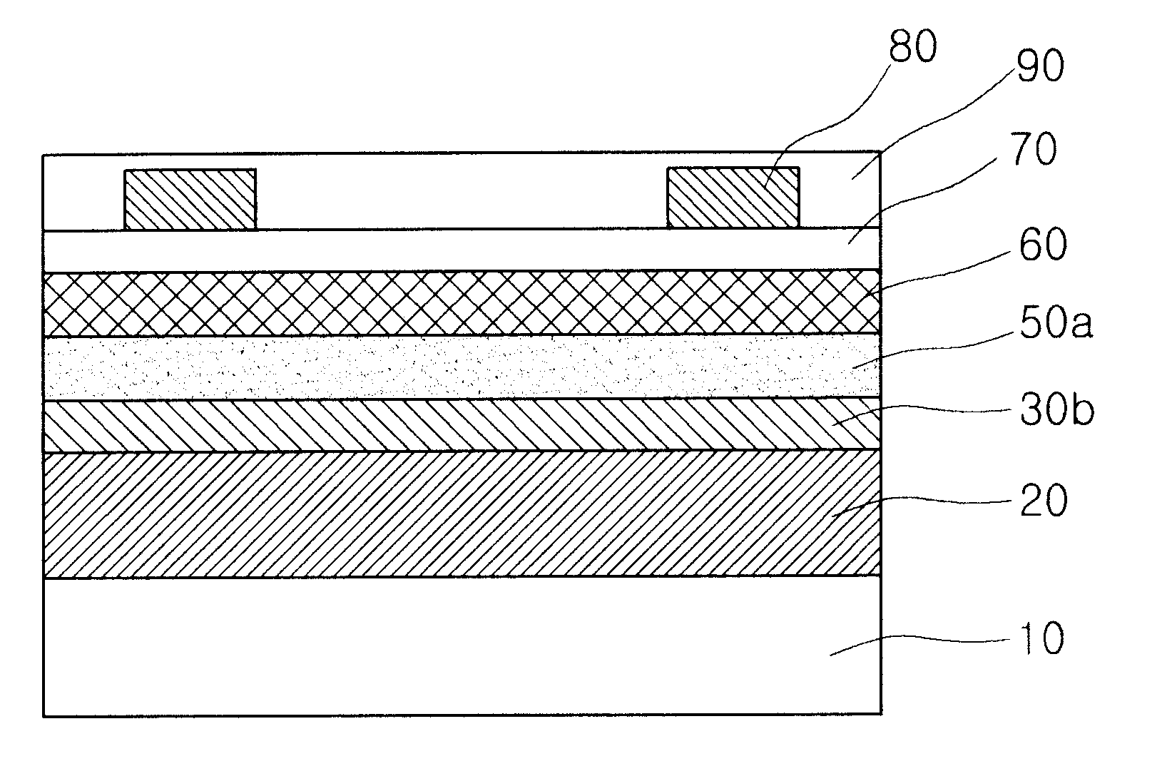
[0050]FIG. 3K is a sectional view showing a polycrystalline silicon solar cell according to an embodiment of the present invention.

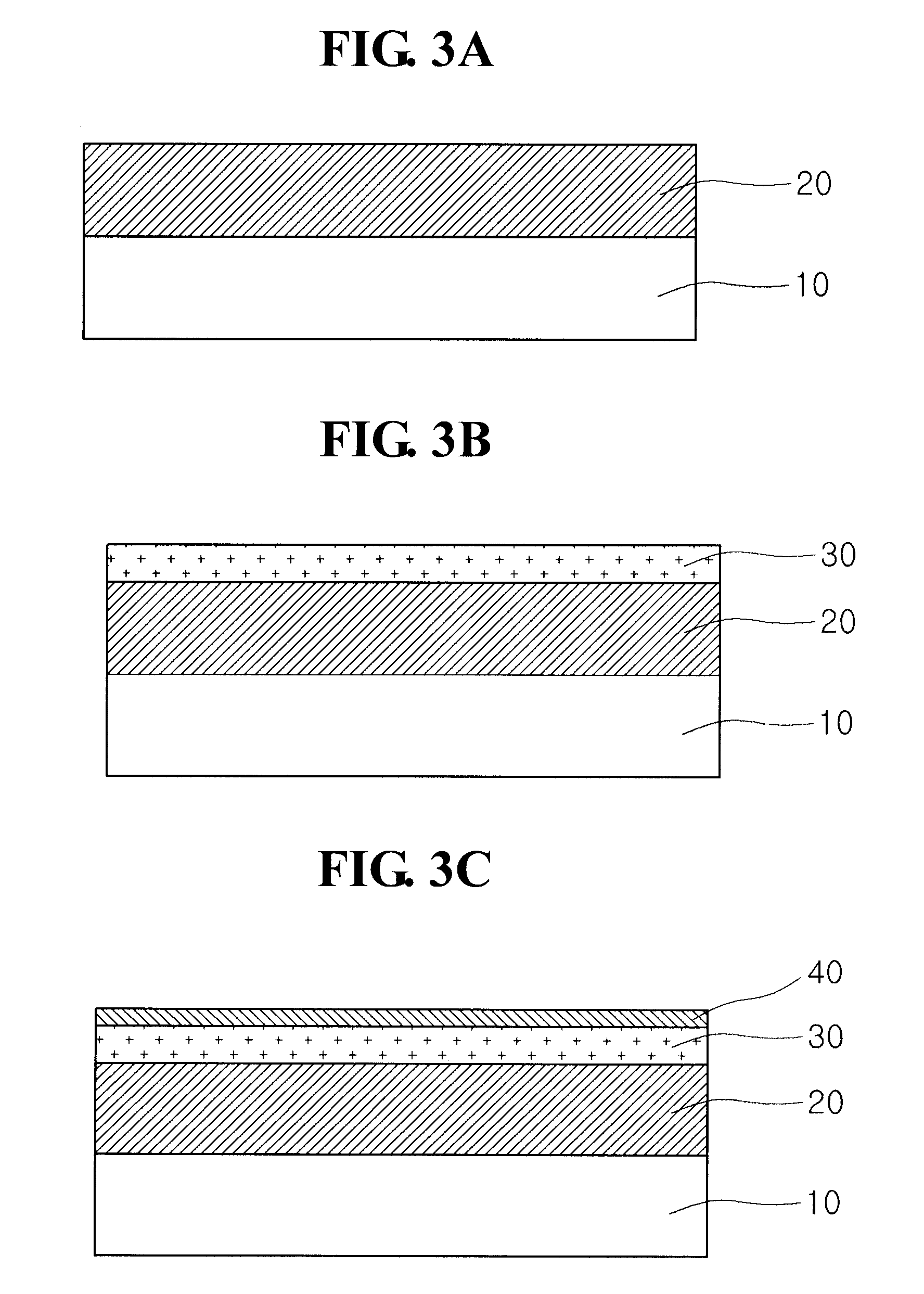
[0051]The polycrystalline silicon solar cell according to an embodiment of the present invention includes: a back electrode 20 formed on a transparent insulating substrate 10; an N-type polycrystalline silicon layer 30b, which is formed on the back electrode 20, in which amorphous silicon is crystallized through a metal induced crystallization (MIC) process, and in which electr...


PUM


Abstract

Disclosed herein is a polycrystalline silicon solar cell, including: a back electrode formed on a transparent insulating substrate; an N-type polycrystalline silicon layer in which amorphous silicon is crystallized through MIC process, and in which electrons are accumulated; a light-absorbing layer which is formed by vertically crystallizing an intrinsic amorphous silicon layer using the polycrystalline silicon layer as a seed for crystallization through MIVC process, in which pairs of electrons and holes are generated in response to incident light, and which has a vertical column grain structure in which grains are arranged in the direction in which electrons and holes move; a P-type polycrystalline silicon layer which has the vertical column grain structure, and in which holes are accumulated; a transparent electrode layer; front electrodes; and an antireflection coating film, and is a method of fabricating the same.

Description

BACKGROUND OF THE INVENTION[0001]1. Field of the Invention[0002]The present invention relates to a polycrystalline silicon solar cell having a high efficiency and a method of fabricating the same, and, more particularly, to a method of forming a light-absorbing layer of a polycrystalline silicon solar cell, in which the light-absorbing layer is formed of non-polluted polycrystalline silicon using a metal-induced lateral crystallization (MILC) process, and grains of the polycrystalline silicon are vertically grown in the direction in which electrons and holes move using a metal-induced vertical crystallization (MIVC) process in which the polycrystalline silicon is used as a crystallization seed, so that the particle structure of the polycrystalline silicon is formed into a vertical columnar structure, with the result that the number of grain boundaries, acting as sites in which electrons and holes are recombined with each other, is minimized, thereby increasing the efficiency of a so...

Claims


Application Information

Patent Timeline
Patent Type & Authority Applications(United States)
IPC IPC(8): H01L31/0368H01L31/18
CPCH01L21/02532H01L21/02672Y02E10/546H01L31/03682H01L31/035281H01L31/0224H01L31/04H01L31/18
Inventor JOO, SEUNG KIYOO, HYEONG SUKKIM, YOUNG SUSONG, NAM KYU
Owner SEOUL NAT UNIV R&DB FOUND
Why Eureka
Try Eureka