Electronic display including a light-emitting element and a color filter sandwiched between two polarizers

a technology of light-emitting elements and color filters, applied in the field of electronic devices, can solve the problems of difficult to take advantage of portable electronic devices in their usability in any place, and easily recognized, and achieve the effects of reducing the weight of light-emitting devices, uniform luminance variations with the passage of time, and enlarging an area capable of displaying images

Inactive Publication Date: 2009-07-16
SEMICON ENERGY LAB CO LTD
View PDF92 Cites 27 Cited by
  • Summary
  • Abstract
  • Description
  • Claims
  • Application Information

AI Technical Summary

Benefits of technology

[0018]By using the light emitting device of the invention which is capable of performing display on both screen sides, downsizing and weight saving of the light emitting device can be achieved while enlarging an area capable of displaying an image. A full color display through the use of a color filter is the existing technology which has been established in a liquid crystal display, and it has the advantage of being applied to a light emitting device easily. Further, it has another advantage that a fine selective coating of an electroluminescent material with a shadow mask is not required as compared to a method of performing a full color display by using light emitting elements corresponding to three primary colors, thus luminance variations with the passage of time is uniform among all the colors. There is no concern as in the case of a CCM method in which blue light is converted into green or red light by using a color conversion material formed of a fluorescent material, that purity of red color is decreased due to a low color conversion efficiency, or a pixel emits light due to the outside light such as sunlight because of the color conversion material itself being a fluorescent body, which may otherwise lower contrast.

Problems solved by technology

Meanwhile, in the case of a reflective type which utilizes the outside light, an image cannot be recognized easily in a dark place, which makes it difficult to take advantage of a portable electronic apparatus in its usability in any place.

Method used


Image

  • Electronic display including a light-emitting element and a color filter sandwiched between two polarizers
  • Electronic display including a light-emitting element and a color filter sandwiched between two polarizers
  • Electronic display including a light-emitting element and a color filter sandwiched between two polarizers

Examples


embodiment mode 1

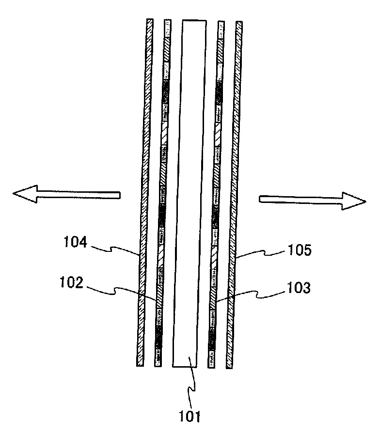
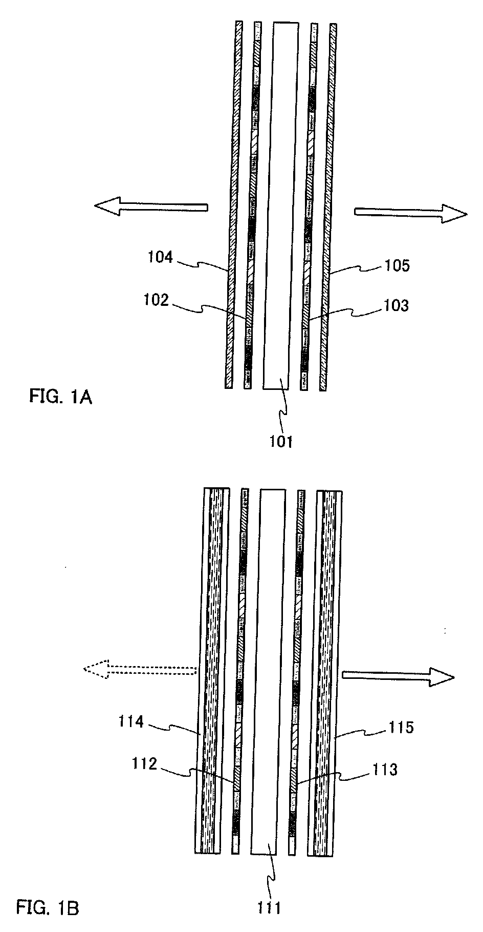
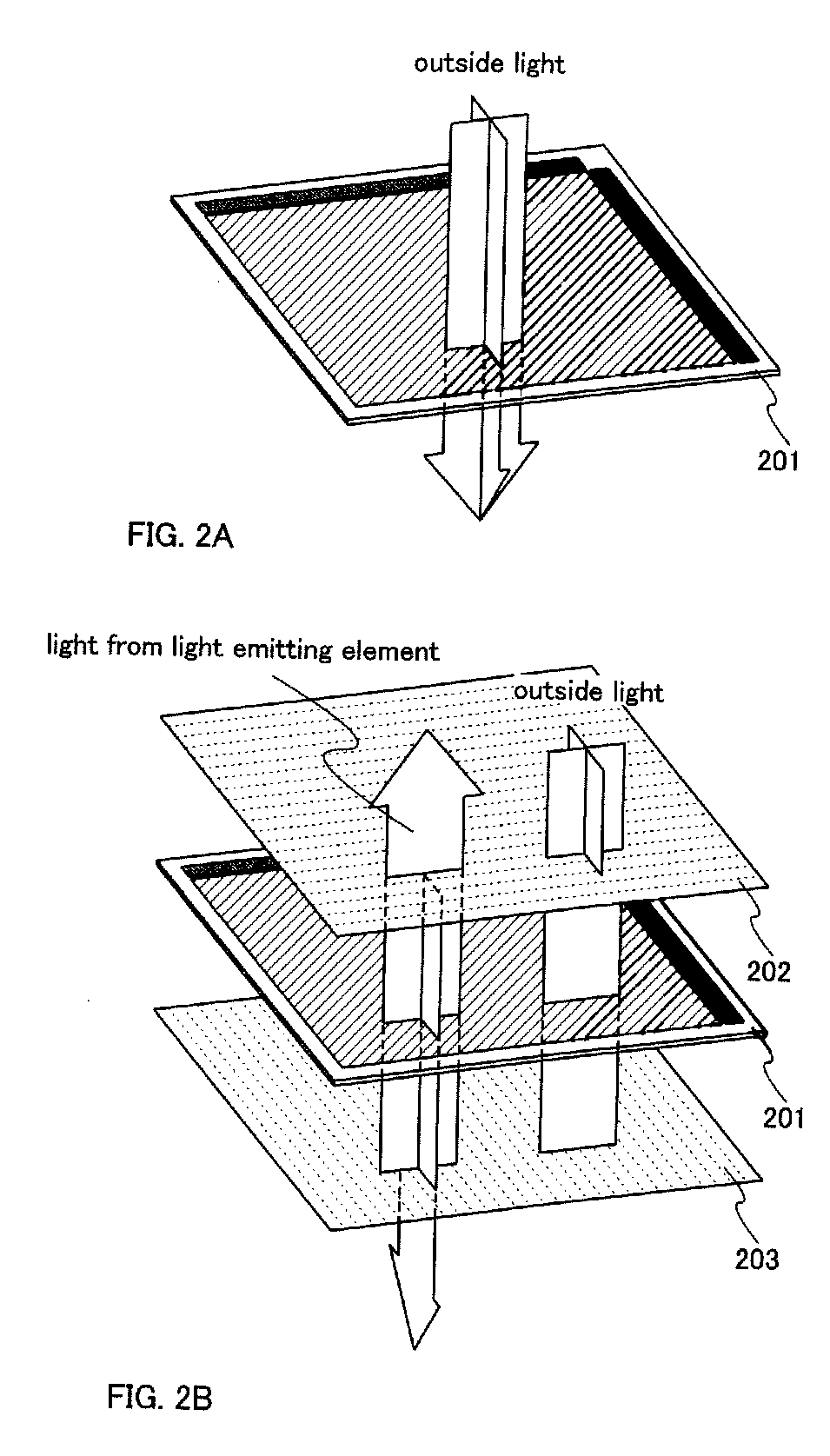
[0020]A specific structure of the invention is described with reference to FIG. 1. FIG. 1A shows one mode of a cross sectional structure of the light emitting device of the invention. The light emitting device of the invention shown in FIG. 1A includes a light emitting panel 101 in which a light emitting element is disposed in each pixel, two color filters 102 and 103 sandwiching the light emitting panel 101, and two polarizers 104 and 105 sandwiching the light emitting panel 101 and the color filters 102 and 103.

[0021]The light emitting panel 101 has a structure in which light from the light emitting element is emitted to the both sides as shown by hollow arrows. Specifically, each light emitting element employs an electrode having a light transmitting characteristic (light transmissivity) as an anode and a cathode. The light emitting element is characterized by emitting white light. Among the light emitted from both sides of the light emitting panel 101, light having a wavelength ...

embodiment mode 2

[0033]FIG. 4A shows one mode of a pixel of the light emitting device of the invention. The pixel shown in FIG. 4A includes a light emitting element 401, a transistor (switching transistor) 402 used as a switching element for controlling an input of a video signal to the pixel, a driving transistor 403 for controlling a current value supplied to the light emitting element 401, and a current controlling transistor 404 for selecting whether or not to supply a current to the light emitting element 401. Further, a capacitor 405 for storing a potential of a video signal may be provided in the pixel as in this embodiment mode.

[0034]The driving transistor 403 and the current controlling transistor 404 have the same polar character In FIG. 4A, both of them are of a P-type, however, they may be of an N-type. According to the invention, the driving transistor 403 operates in a saturation region while the current controlling transistor 404 operates in a linear region. A channel length L of the ...

embodiment mode 3

[0046]In this embodiment mode, one mode of a pixel of the light emitting device of the invention is described, which is different from that in FIG. 4A.

[0047]The pixel shown in FIG. 4B includes a light emitting element 411, a switching transistor 412, a driving transistor 413, a current controlling transistor 414, and a transistor (erasing transistor) 416 for erasing a potential of a written video signal. Further, a capacitor 415 may be provided in the pixel in addition to the above elements. The driving transistor 413 and the current controlling transistor 414 have the same polar character. According to the invention, the driving transistor 413 operates in a saturation region while the current controlling transistor 414 operates in a linear region. L of the driving transistor 413 may be longer than W thereof. L of the current controlling transistor 414 may be equal to or shorter than W thereof. The ratio of L to W of the driving transistor 413 is desirably five or more.

[0048]The dri...


PUM

PropertyMeasurementUnit
deflection anglesaaaaaaaaaa
thickaaaaaaaaaa
thicknessaaaaaaaaaa

Abstract

It is an object of the invention to achieve weight saving and downsizing of an electronic apparatus, in particular a portable electronic apparatus while enlarging a display screen thereof. The invention provides an electronic apparatus using a light emitting device which includes a light emitting element, a color filter provided on either side of an anode or a cathode of the light emitting element, and two polarizers sandwiching the light emitting element and the color filter, in which the anode and the cathode transmit light, deflection angles of the two polarizers are different from each other, and light obtained from the light emitting element is white.

Description

CROSS-REFERENCE TO RELATED APPLICATIONS[0001]This application is a divisional of U.S. application Ser. No. 10 / 816,185, filed Apr. 2, 2004, now pending, which claims the benefit of a foreign priority application filed in Japan as Serial No. 2003-103114 on Apr. 7, 2003, both of which are incorporated by reference.TECHNICAL FIELD[0002]The present invention relates to an electronic apparatus using a light emitting device, and more particularly to a portable electronic apparatus.BACKGROUND ART[0003]Portable electronic apparatuses typified by a portable phone, an electronic databook, and the like have been required to be equipped with various functions such as transmission / reception of e-mail, voice recognition, image pickup with a small-size camera as well as a display device for displaying images, while there have been strong demand of users for downsizing and weight saving. Therefore, it is required that the larger number of ICs having a larger circuit scale and higher memory capacity ...

Claims


Application Information

Patent Timeline
Patent Type & Authority Applications(United States)
IPC IPC(8): H01J1/62G02F1/01H05B33/22G09F9/30G09G3/32H01L27/32H01L51/50H01L51/52H05B33/00H05B33/14
CPCG09G2310/0251H01L27/322H01L27/3246H01L51/5016H01L51/5036G09G2300/0842H01L2251/5323G02F1/133603G02F2001/133342G09G3/3225G09G2300/046H01L51/5281G02F1/133342H10K59/38H10K59/122H10K50/125H10K50/11H10K2101/10H10K2102/3031H10K59/8791A47J36/06A47J27/56H10K50/86
Inventor ABE, HIROKOOSAME, MITSUAKIANZAI, AYAYAMAZAKI, YUTANADA, YOSHIFUMIYAMAZAKI, SHUNPEI
Owner SEMICON ENERGY LAB CO LTD
Why Eureka
Try Eureka