Two-wavelength semiconductor laser device and its fabricating method

a two-wavelength semiconductor and laser device technology, applied in semiconductor lasers, laser details, nanooptics, etc., can solve the problems of deterioration of current-light characteristics due to carrier absorption or cod at low light output, disadvantages of window structure, and insufficient provision of cladding layer made of algainp mixed crystal to achieve higher power of cd semiconductor laser devices. , to achieve the effect of less light absorption, low cost and simple process

Active Publication Date: 2009-07-16
PANASONIC SEMICON SOLUTIONS CO LTD
View PDF13 Cites 7 Cited by
  • Summary
  • Abstract
  • Description
  • Claims
  • Application Information

AI Technical Summary

Benefits of technology

[0050]According to the integrated two-wavelength semiconductor laser device and its fabricating method of the present invention, the band gap of the facet window structure can be caused to be large without introducing an excessive amount of impurity to the quantum well active layer, and the window structure having less light absorption can be formed at the facets of both the semiconductor lasers with a simple process. Therefore, an integrated two-wavelength semiconductor laser device capable of a high-power operation can be provided with low cost.

Problems solved by technology

It was found that the provision of the cladding layer made of AlGaInP mixed crystal is not sufficient to achieve higher power of the CD semiconductor laser device.
However, in the CD semiconductor laser device, the excessive impurity diffusion causes diffusion of constituent elements from AlGaInP crystal of the cladding layer, so that the resultant disordered crystal has a smaller band gap than that of the average composition of the well layer and the barrier layers sandwiching the well layer, which is disadvantageous to the window structure.
Specifically, it was found that the influence of undesired diffusion of elements constituting the cladding layer or an excess of an impurity leads to occurrence of a crystal defect, or the above-described difference in diffusion coefficient leads to occurrence of pileup of an impurity to the quantum well active layer, so that light absorption due to free carriers increases, and therefore, a deterioration in current-light characteristics due to carrier absorption or COD at low light output may occur.
Similarly, it was found that, also in the DVD semiconductor laser device, although both the quantum well active layer and the cladding layer are made of AlGaInP crystal, excessive impurity diffusion causes a deterioration in current-light characteristics or occurrence of COD at low light output.

Method used


Image

  • Two-wavelength semiconductor laser device and its fabricating method
  • Two-wavelength semiconductor laser device and its fabricating method
  • Two-wavelength semiconductor laser device and its fabricating method

Examples


first embodiment

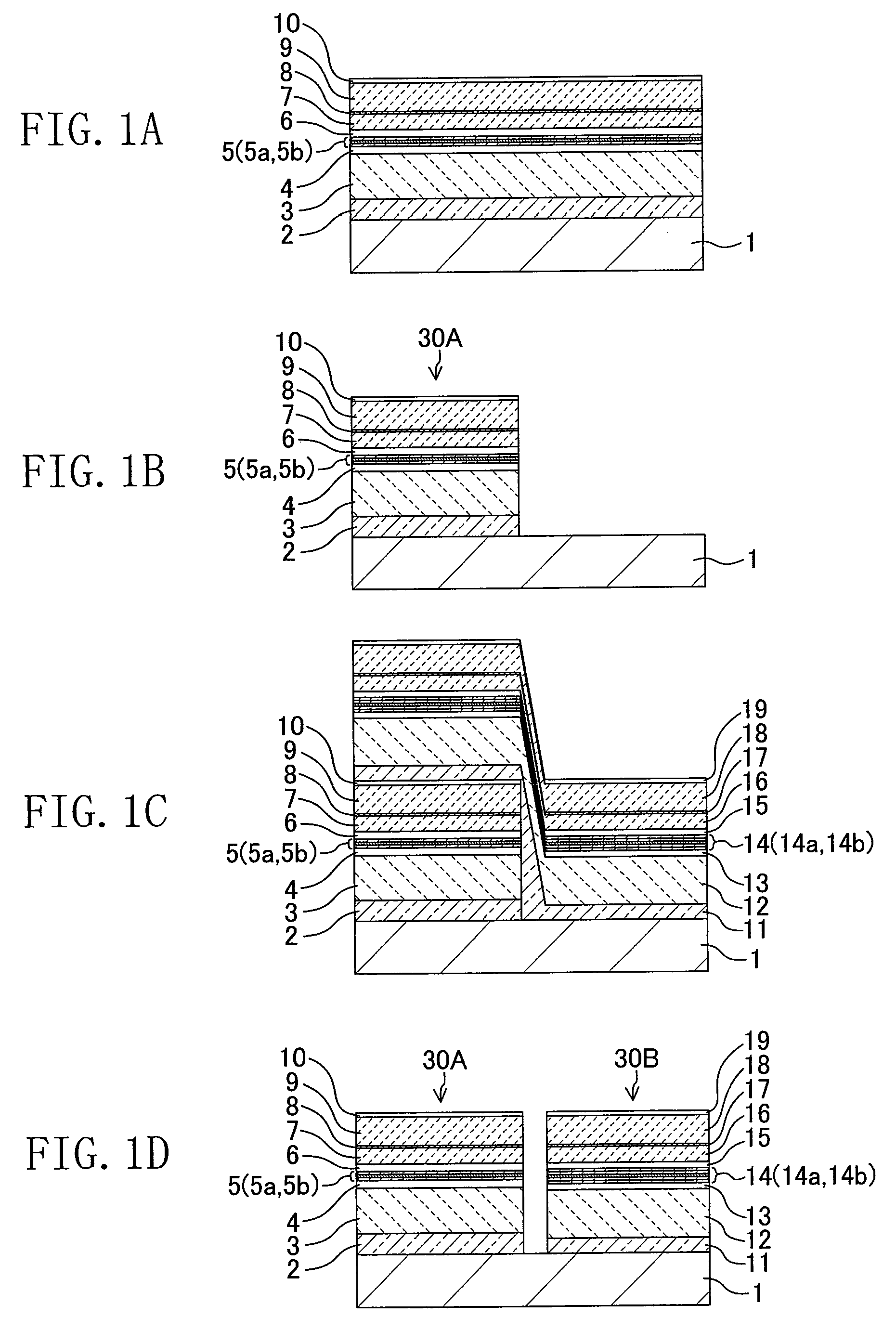
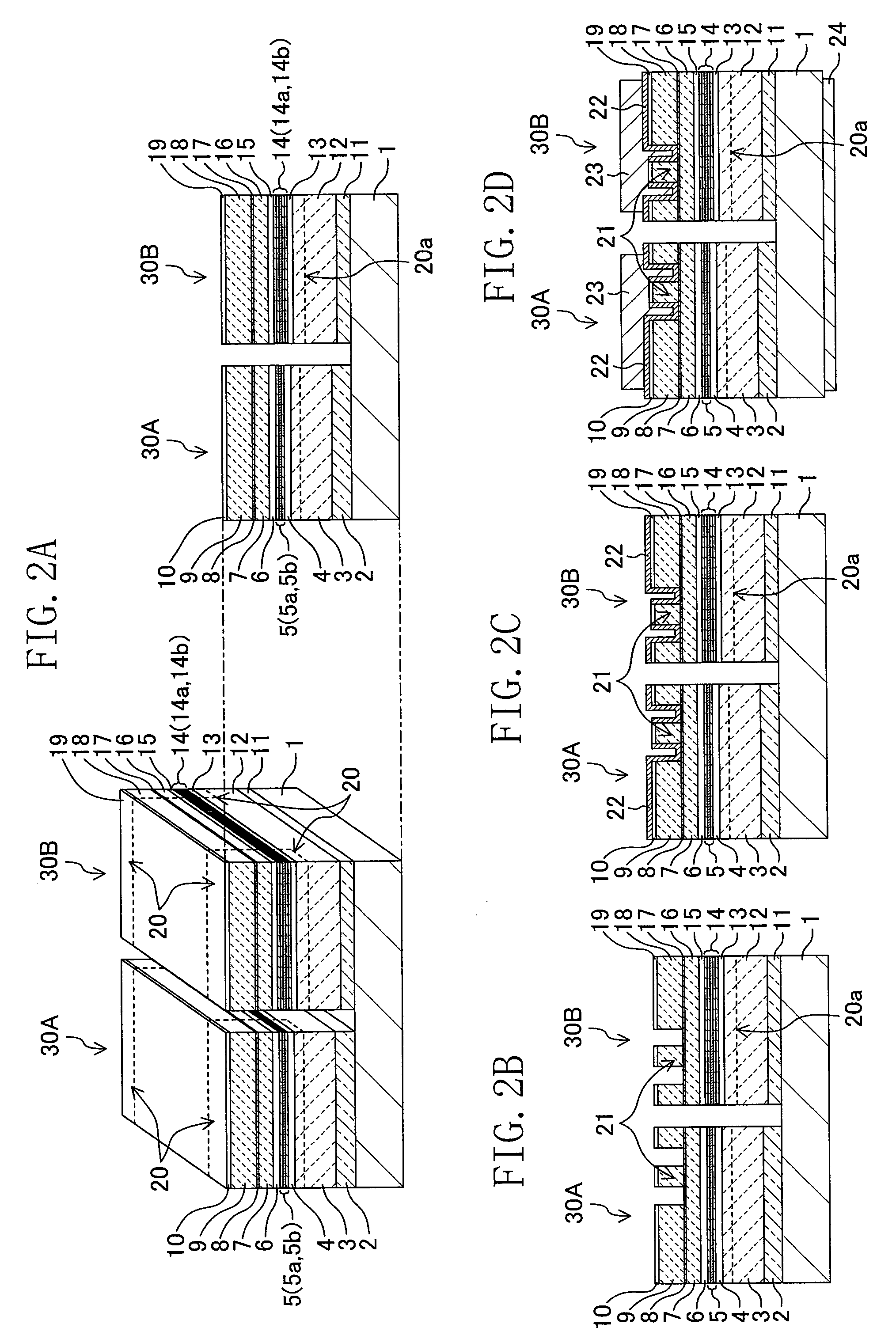
[0063]Hereinafter, an integrated two-wavelength semiconductor laser device according to a first embodiment of the present invention and its fabricating method will be described.

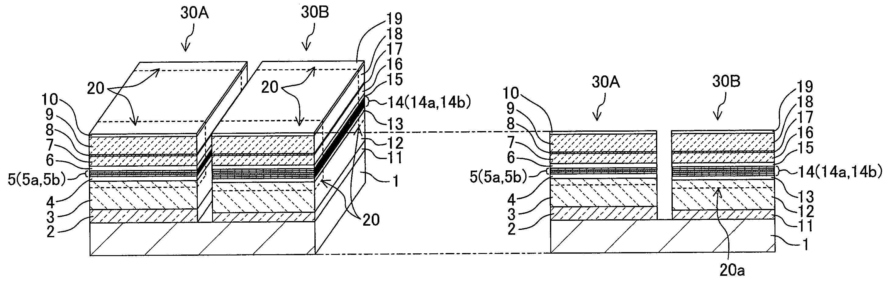
[0064]FIGS. 1A to 1C and FIGS. 2A to 2D are cross-sectional views showing steps of fabricating the integrated two-wavelength semiconductor laser device of the first embodiment of the present invention in sequence. It is hereinafter assumed that, for example, a two-wavelength semiconductor laser device is fabricated in which a first semiconductor laser device 30A that is, for example, a semiconductor laser for CDs (oscillation wavelength: 760 nm or more and 790 nm or less (760 nm to 790 nm)) and a second semiconductor laser device 30B that is, for example, a semiconductor laser for DVDs (oscillation wavelength: 650 nm or more and 670 nm (650 nm to 670 nm)) are monolithically integrated on a substrate.

[0065]Initially, as shown in FIG. 1A, a crystal growing device (e.g., MOCVD, etc.) is used to deposit, on a sub...

second embodiment

[0110]Hereinafter, an integrated two-wavelength semiconductor laser device according to a second embodiment of the present invention and its fabricating method will be described.

[0111]FIGS. 8A to 8D and FIGS. 9A to 9C are cross-sectional views showing steps of fabricating the integrated two-wavelength semiconductor laser device of the second embodiment of the present invention in sequence. As in the first embodiment, it is hereinafter assumed that, for example, a two-wavelength semiconductor laser device is fabricated in which a first semiconductor laser device 30C that is, for example, a semiconductor laser for CDs (oscillation wavelength: 760 nm to 790 nm) and a second semiconductor laser device 30B that is, for example, a semiconductor laser for DVDs (oscillation wavelength: 650 nm to 670 nm) are monolithically integrated on a substrate.

[0112]Initially, as shown in FIG. 8A, a crystal growing device (e.g., MOCVD, etc.) is used to deposit, on a substrate 1 made of n-type GaAs that ...


PUM


Abstract

A two-wavelength semiconductor laser device includes a first semiconductor laser device including a first-conductivity type first cladding layer, a first guide layer made of AlGaAs mixed crystal, a first quantum well active layer having a barrier layer made of AlGaAs mixed crystal, a second guide layer made of AlGaAs mixed crystal, and a second-conductivity type second cladding layer, and a second semiconductor laser device including a first-conductivity type third cladding layer, a third guide layer made of AlGaInP mixed crystal, a second quantum well active layer having a barrier layer made of AlGaInP mixed crystal, a fourth guide layer made of AlGaInP mixed crystal, and a second-conductivity type fourth cladding layer. At least the barrier layer included in the first quantum well active layer, the first guide layer, and the second guide layer each have an Al molar ratio of more than 0.47 and 0.60 or less.

Description

BACKGROUND OF THE INVENTION[0001]1. Field of the Invention[0002]The present invention relates to a red (oscillation wavelength: 650-nm band) and infrared (oscillation wavelength: 780-nm band) integrated high-power two-wavelength semiconductor laser device that is used as, for example, a light source for a pickup of an optical disc device, a light source for other electronic devices and information processing devices, or the like, and a method for fabricating the two-wavelength semiconductor laser device.[0003]2. Description of the Related Art[0004]On the current market, there are a large-capacity Digital Video Disc (DVD) capable of high-density recording and various DVD devices that record and reproduce the disc. Taking it into account how popular DVD devices have become (e.g., DVD devices are becoming widespread as DVD recorders in homes and are often supplied as standard equipment to personal computers), the demand is expected to increase more and more in the future. On the other ...

Claims


Application Information

Patent Timeline
Patent Type & Authority Applications(United States)
IPC IPC(8): H01S5/00H01L21/00
CPCB82Y20/00H01S5/162H01S5/2004H01S5/2201H01S5/2231H01S2301/185H01S5/34313H01S5/34326H01S5/4031H01S5/4087H01S5/3202
Inventor MAKITA, KOUJIKASHIMA, TAKAYUKI
Owner PANASONIC SEMICON SOLUTIONS CO LTD
Why Eureka
Try Eureka