Methods for forming a composite pattern including printed resolution assist features

a composite pattern and assist feature technology, applied in the field of semiconductor processing methods, can solve the problems of high undesirable alcohol based photoresist in the manufacturing facility, inability to be done, and inability to use conventional organic-based single layer photoresist or inorganic hardmasks, so as to improve the printability, the effect of increasing the printability of the first pattern

Inactive Publication Date: 2009-07-16
TAIWAN SEMICON MFG CO LTD
View PDF13 Cites 23 Cited by
  • Summary
  • Abstract
  • Description
  • Claims
  • Application Information

AI Technical Summary

Benefits of technology

[0032]In one embodiment, printability of the first-pattern is greater than printability of the first sub-pattern. For example, the printability of the first pattern may be greater than the printability if the first-sub pattern by containing a more periodic structure than the first sub-pattern. Such improvement in the printability may be achieved when instances of the unit pattern is present in the first pattern, while the first sub-pattern and the second sub-pattern do not contain any instance of the unit pattern.

Problems solved by technology

However, many solutions that have been developed for enhancing the process window of layers such and contract holes or metal lines (which require resist holes and / or trenches) with clear PRAFs have drawbacks, Dah-Chung Owe-Yang et al.
These alcohol based photoresist are highly undesirable in a manufacturing facility.
This can usually not be done since the extra features interfere with the functionality of the chip.
herefore, a conventional organic-based single layer photoresist or an inorganic hardmask may not be employed according to this method.

Method used


Image

  • Methods for forming a composite pattern including printed resolution assist features
  • Methods for forming a composite pattern including printed resolution assist features
  • Methods for forming a composite pattern including printed resolution assist features

Examples


Embodiment Construction

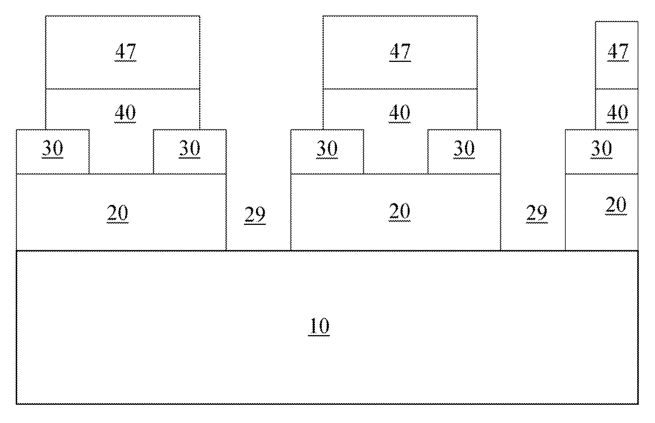
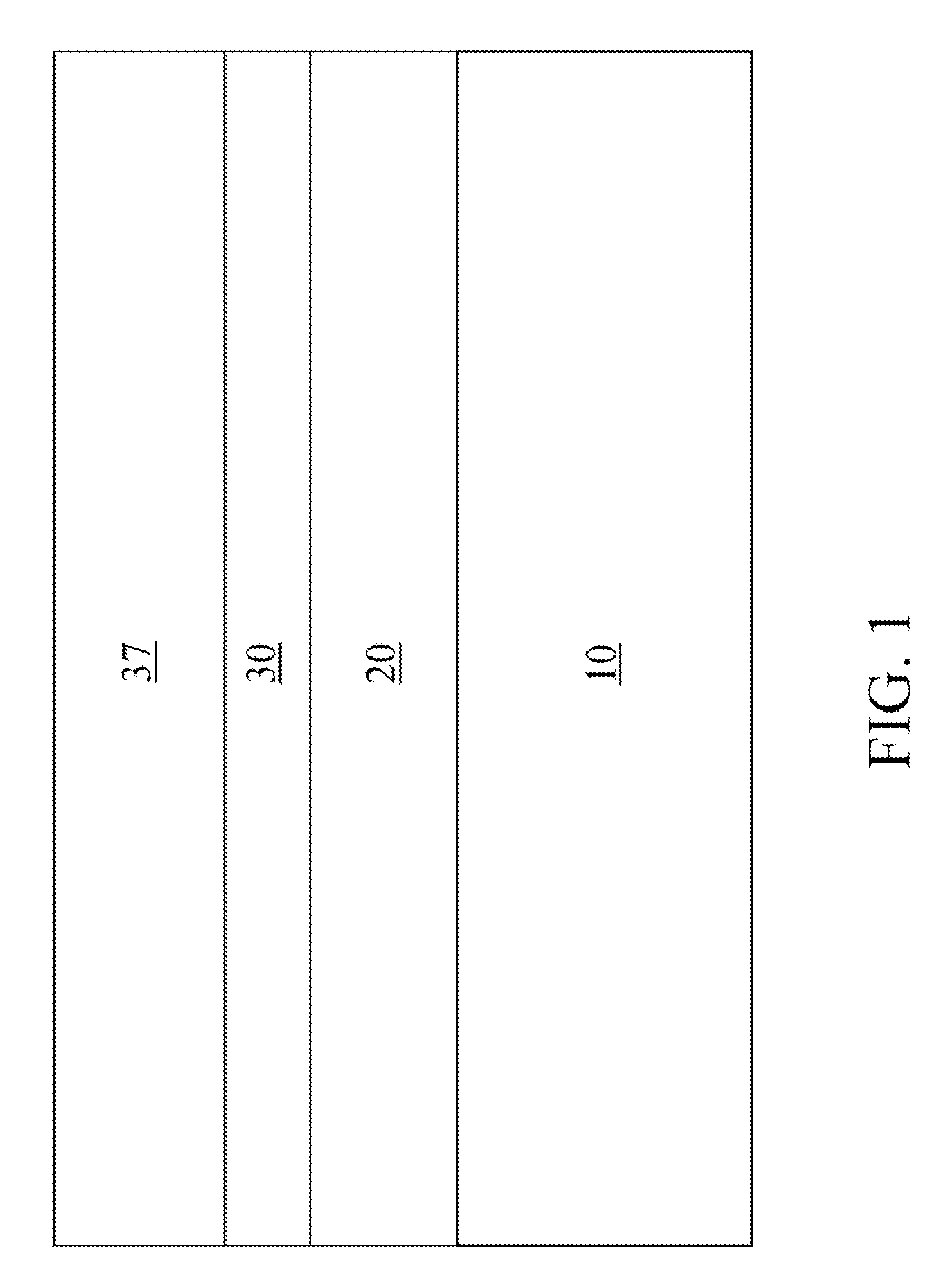
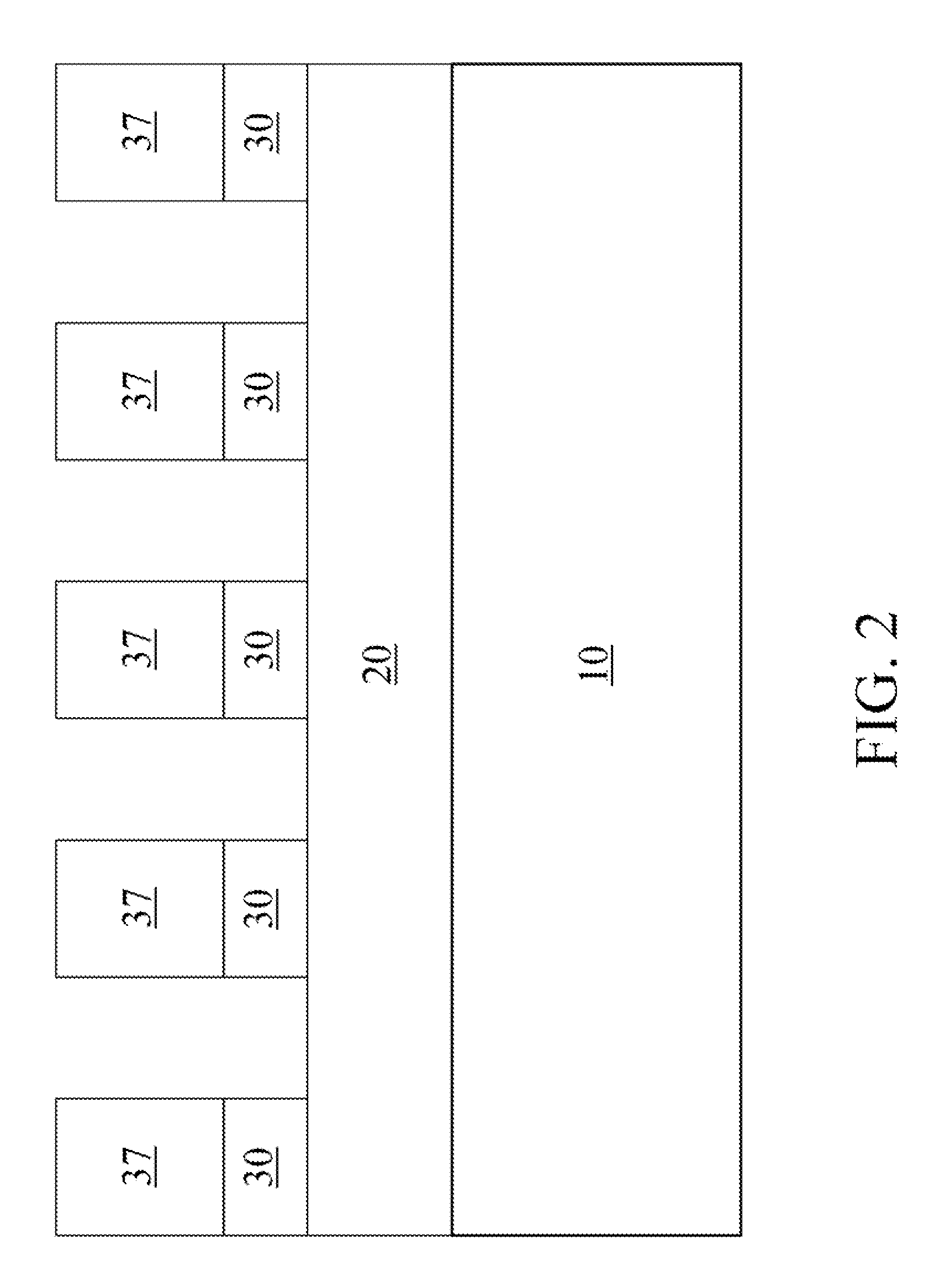
[0059]As stated above, the present invention relates to methods for forming a composite lithographic pattern of two lithographic patterns employing clear printed resolution assist features (cPRAFs) and a hard mask layer, which are now described in detail with accompanying figures. It is noted that like and corresponding elements are referred to by like reference numerals.

[0060]In the present invention, methods for forming a composite lithographic pattern of a first and second pattern is provided, wherein the first pattern has a first sub-pattern that contains the features that need to be created based on the design and a second sub-pattern of clear printed resolution assist features (cPRAFs). In this invention, the printability of the first sub-pattern is enhanced by the co-patterning with the second sub-pattern (cPRAFs). The printability here refers to quality of the aerial image contrast, or the profile gradient of a feature edge, which can be determined by a number of standard me...


PUM

PropertyMeasurementUnit
thicknessesaaaaaaaaaa
anisotropicaaaaaaaaaa

Abstract

An underlayer to be patterned with a composite pattern is formed on a substrate. The composite pattern is decomposed into a first pattern and a second pattern, each having reduced complexity than the composite pattern. A hard mask layer is formed directly on the underlying layer. A first photoresist is applied over the hard mask layer and lithographically patterned with the first pattern, which is transferred into the hard mask layer by a first etch. A second photoresist is applied over the hard mask layer. The second photoresist is patterned with the second pattern to expose portions of the underlying layer. The exposed portions of the underlying layer are etched employing the second photoresist and the hard mask layer, which contains the first pattern so that the composite pattern is transferred into the underlying layer.

Description

FIELD OF THE INVENTION[0001]The present invention relates to semiconductor processing methods, and particularly to methods for forming a composite lithographic pattern of two lithographic patterns employing clear printed resolution assist features (cPRAF) and a hard mask layer.BACKGROUND OF THE INVENTION[0002]As the minimum pitch required to be resolved has decreased more aggressive off-axis illuminations have been required. These aggressive illuminations allow the minimum pitch to be resolved but have also decreased the depth of focus of larger pitches (typically pitches 1.5 times the minimum pitch). One of the methods employed to improve printability and image fidelity of features with pitches greater than minimum is use of printed resolution assist feature (PRAF), which has dimensions greater or equal to that of the minimum feature size. The difference between a PRAF and a sub-resolution assist feature (SRAF) is that the dimensions of the PRAF are large enough that they are resol...

Claims


Application Information

Patent Timeline
Patent Type & Authority Applications(United States)
IPC IPC(8): G03F7/20
CPCG03F7/70433H01L21/0337G03F7/70466
Inventor GABOR, ALLEN H.HALLE, SCOTT D.WANG, HELEN
Owner TAIWAN SEMICON MFG CO LTD
Why Eureka
Try Eureka