

Photoelectric conversion element and solid-state imaging device
- Summary
- Abstract
- Description
- Claims
- Application Information
AI Technical Summary
Benefits of technology
Problems solved by technology
Method used
Image

Examples
first embodiment
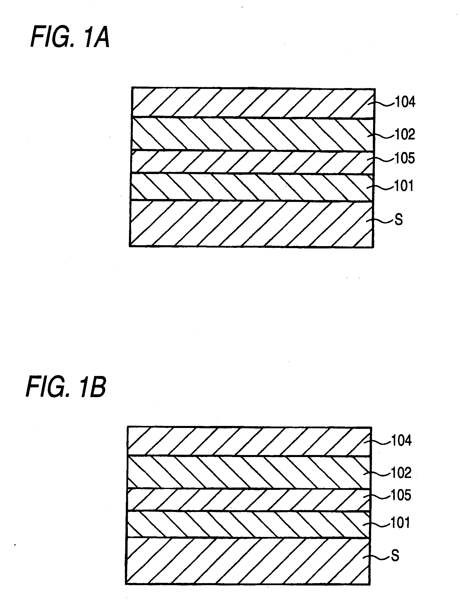
[0033]FIG. 1A is a schematic cross-sectional view showing the fundamental structure of a photoelectric conversion element of a first exemplary embodiment of the invention. Also, FIG. 1B is a schematic cross-sectional view showing a modified example of the photoelectric conversion element of the first embodiment.
[0034]The photoelectric conversion element shown in FIG. 1A includes a substrate S, a lower electrode (pixel electrode) 101 formed on the substrate S, a hole-blocking layer 105 formed on the lower electrode 101, a photoelectric conversion layer 102 formed on the hole-blocking layer 105, and an upper electrode (opposing electrode) 104 formed on the photoelectric conversion layer 102. Also, the photoelectric conversion element shown by FIG. 1B includes a substrate S, a lower electrode (pixel electrode) 101 formed on the substrate S, an electron-blocking layer 103 formed on the lower electrode 101, a photoelectric conversion layer 102 formed on the electron-blocking layer 103, a...
second embodiment
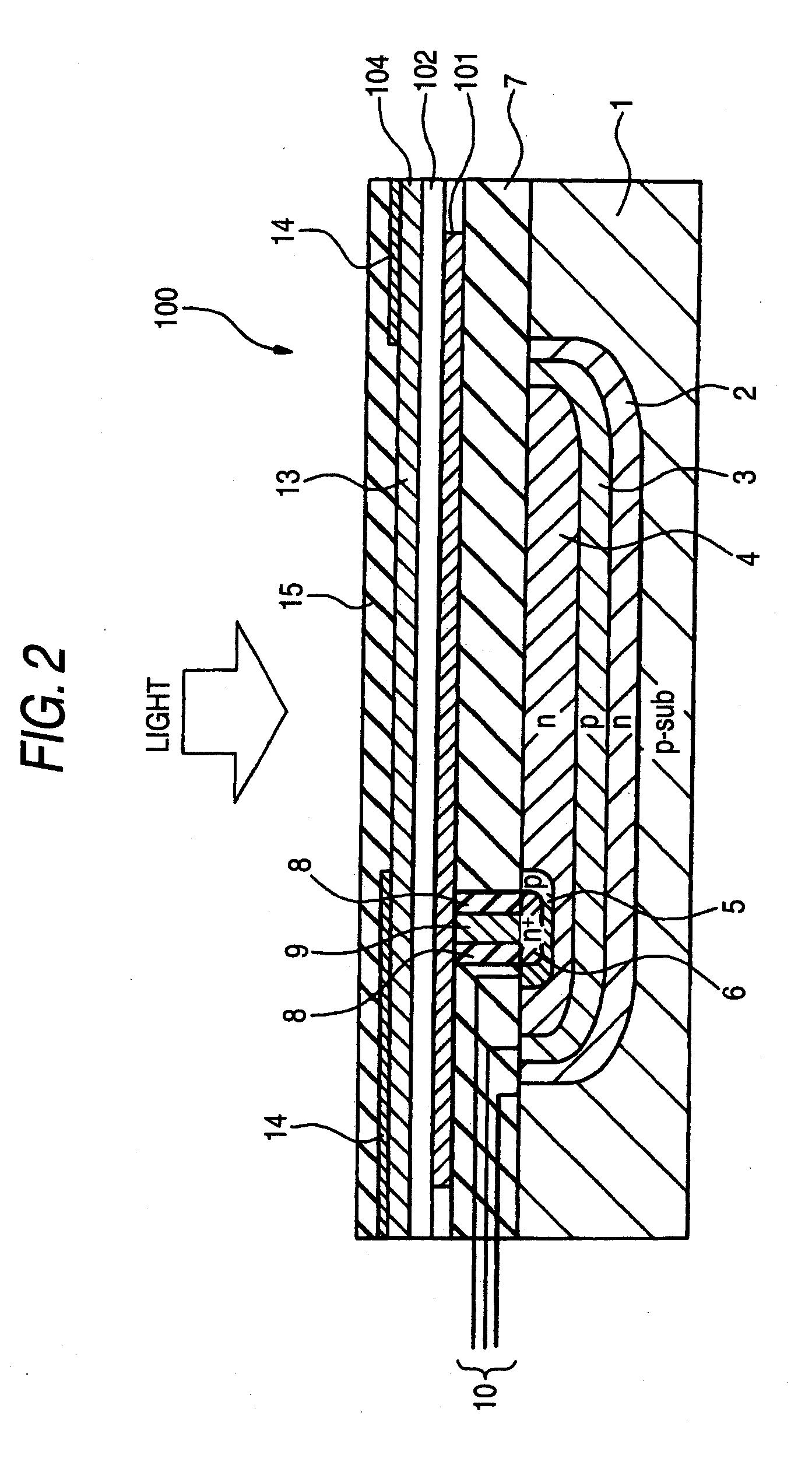
[0086]FIG. 2 is a cross-sectional schematic view showing one pixel of a solid-state imaging device for illustrating a second exemplary embodiment of the invention. In FIG. 2, the same reference numerals and signs are applied to the same structural members as those in FIG. 1.
[0087]In a solid-state imaging device 100, a number of pixels shown in FIG. 2 are arranged on the same plane in an array pattern, and data on one pixel of an image data can be generated by a signal obtained from the one pixel.
[0088]One pixel of the solid-state imaging device shown in FIG. 2 includes a p-type silicon substrate 1, a transparent insulating film 7 formed on the p-type silicon substrate 1, and a photoelectric conversion element of the structure described in the first embodiment comprising a lower electrode 101 formed on the insulating film 7, a photoelectric conversion layer 102 formed on the lower electrode 101, an electron-blocking layer 103 (not shown) formed on the photoelectric conversion layer 1...
third embodiment
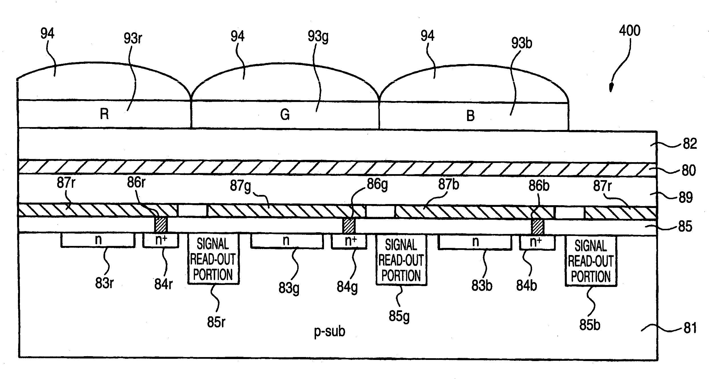
[0096]In this embodiment, two photodiodes are not stacked within the silicon substrate 1 shown in FIG. 2, but are arranged in the vertical direction to the entering direction of the incident light to detect two color lights within the p-type silicon substrate.
[0097]FIG. 3 is a cross-sectional schematic view showing one pixel of a solid-state imaging device for illustrating a third exemplary embodiment of the invention. In FIG. 3, the same reference numerals and signs are applied to the same structural members as those in FIG. 1.
[0098]One pixel of the solid-state imaging device 200 shown in FIG. 3 includes a p-type silicon substrate 17, and a photoelectric conversion element of the structure described in the first embodiment comprising a lower electrode 101 formed above the p-type silicon substrate 17, a photoelectric conversion layer 102 formed on the lower electrode 101, an electron-blocking layer 103 (not shown) formed on the photoelectric conversion layer 102, a hole-blocking lay...
PUM
 Abstract
Description
Claims
Application Information