

Photoelectric conversion element and solid-state imaging device
a conversion element and photoelectric technology, applied in the direction of electrical apparatus, semiconductor devices, organic semiconductor devices, etc., can solve the problems of small reduction in photoelectric conversion efficiency, large photo current/dark current ratio of elements, and inability to obtain large photo current/dark current ratios, etc., to achieve sufficient dark current suppressing effect and high photoelectric conversion efficiency
- Summary
- Abstract
- Description
- Claims
- Application Information
AI Technical Summary
Benefits of technology
Problems solved by technology
Method used
Image

Examples
first embodiment
(First Embodiment)
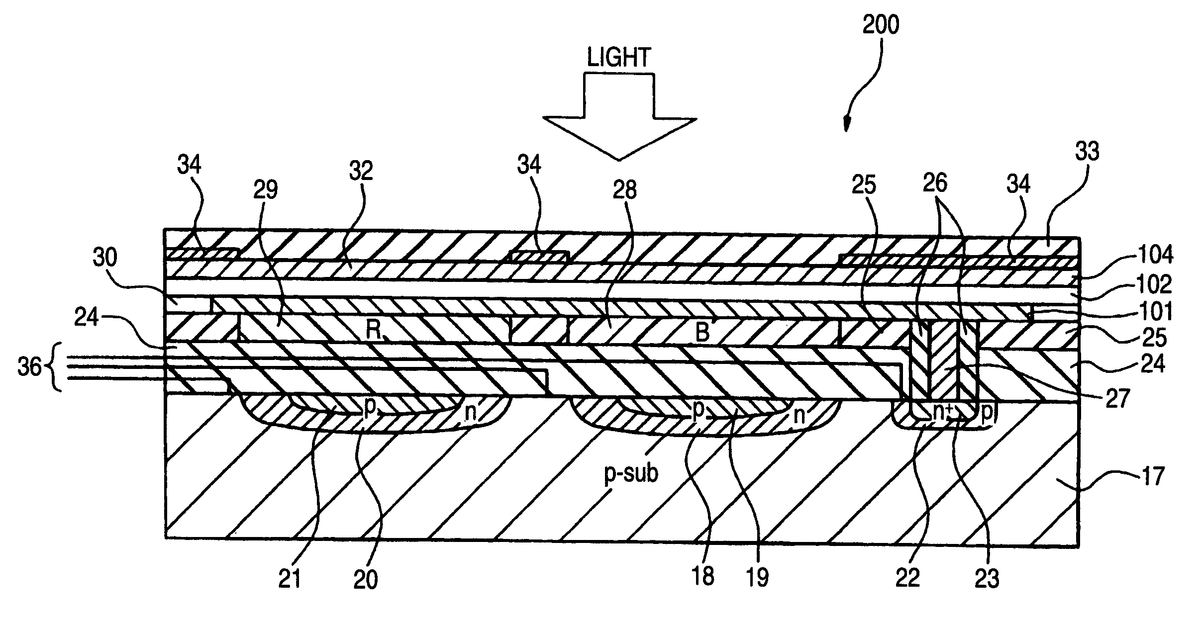
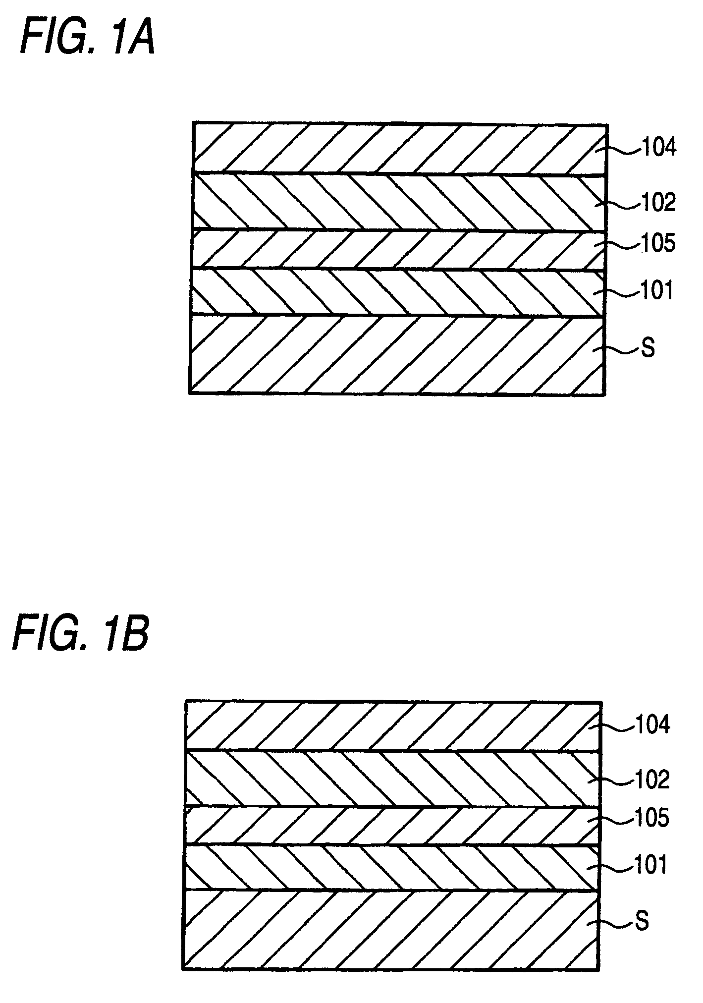
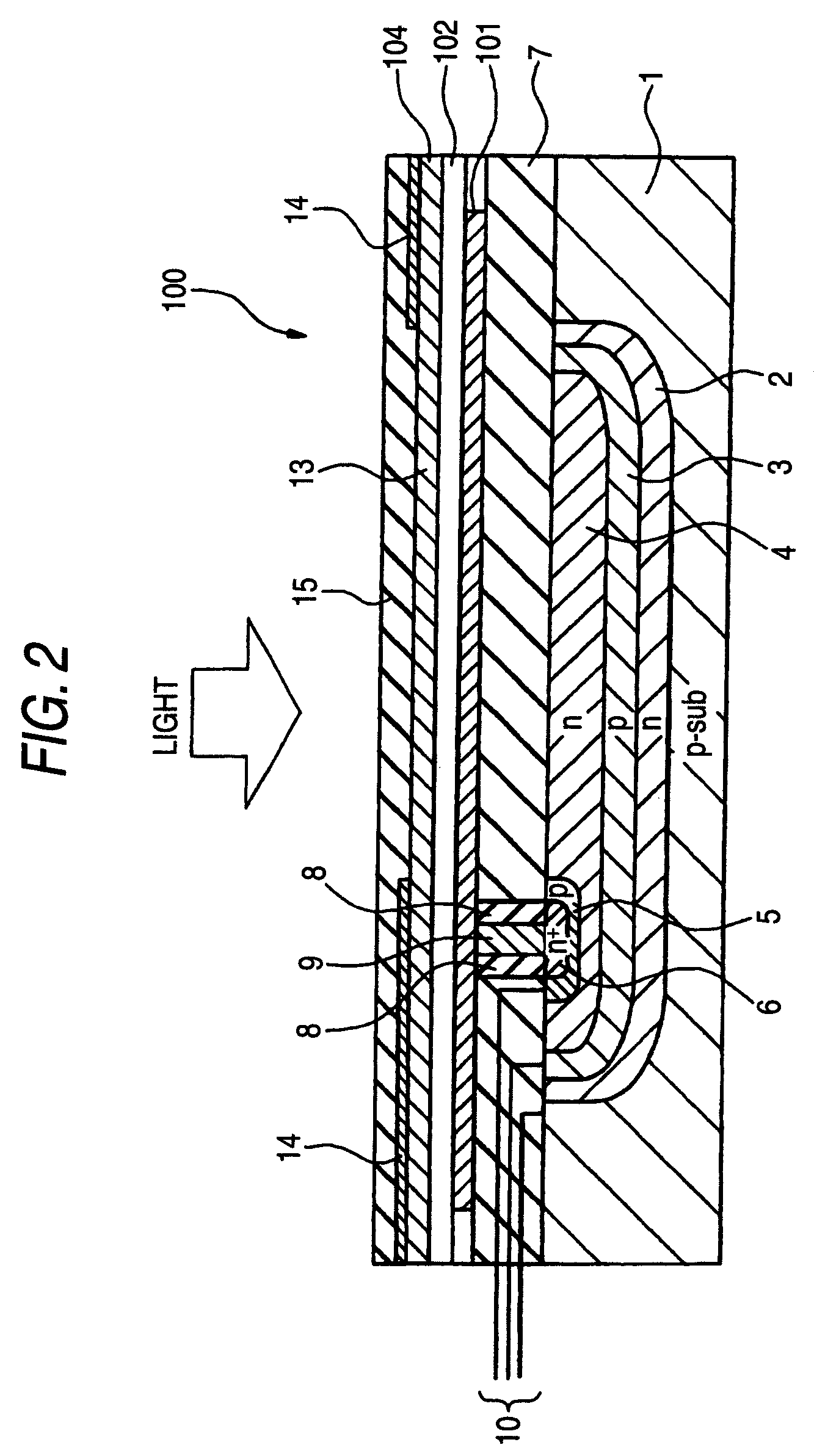
[0050]FIG. 1A is a schematic cross-sectional view showing the fundamental structure of a photoelectric conversion element of a first exemplary embodiment of the invention. Also, FIG. 1B is a schematic cross-sectional view showing a modified example of the photoelectric conversion element of the first embodiment.
[0051]The photoelectric conversion element shown in FIG. 1A includes a substrate S, a lower electrode (pixel electrode) 101 formed on the substrate S, a hole-blocking layer 105 formed on the lower electrode 101, a photoelectric conversion layer 102 formed on the hole-blocking layer 105, and an upper electrode (opposing electrode) 104 formed on the photoelectric conversion layer 102. Also, the photoelectric conversion element shown by FIG. 1B includes a substrate S, a lower electrode (pixel electrode) 101 formed on the substrate S, an electron-blocking layer 103 formed on the lower electrode 101, a photoelectric conversion layer 102 formed on the electron-blo...
example 1
[0178]A 25-mm square glass substrate equipped with an ITO electrode is subjected to ultrasonic cleaning with successive, acetone, Semico Clean, and isopropyl alcohol (IPA), each for 15 minutes. After finally washing with boiling IPA, UV / O3 washing is carried out.
[0179]Next, a hole-blocking layer containing fullerene is formed in a film form on this substrate. As fullerene 60, nanom purpule (C60) manufactured by Frontier Carbon Corporation is used. 2.5 wt % polycarbonate resin PCz (Yupiron PCZ-400; manufactured by Mitsubishi Gas Chemicals Company, Inc.) and 30 wt %, based on PCz, of fullerene C60 are dissolved in o-dichlorobenzene to prepare a coating solution. This coating solution is spin-coated on the glass substrate to form a film, followed by evaporating the solvent in a vacuum drier to form a 1000-{acute over (Å)} thick hole-blocking layer.
[0180]The substrate is then transferred into an organic vacuum deposition chamber and, while rotating the substrate holder, quinacridone (bo...
example 2
[0183]An S / N ratio is calculated in the same manner as in Example 1 except for using fullerene C70 in place of fullerene C60.
PUM
 Abstract
Description
Claims
Application Information