Thin film transistor, method of fabricating the same, and organic light emitting diode display device having the TFT

a technology of thin film transistors and display devices, which is applied in the direction of discharge tubes/lamp details, discharge tubes luminescnet screens, electric discharge lamps, etc., can solve the problems of deformation of substrates, degrading the interfacial characteristics of semiconductor layers, and the spc method takes too much time, so as to improve the electrical properties of tft and reduce the amount of metal catalysts

Active Publication Date: 2009-07-30
SAMSUNG DISPLAY CO LTD
View PDF4 Cites 24 Cited by
  • Summary
  • Abstract
  • Description
  • Claims
  • Application Information

AI Technical Summary

Benefits of technology

[0010]Aspects of the present invention provide a bottom-gate thin film transistor (TFT), a method of fabricating a TFT, and an organic light emitting diode (OLED) display device having the TFT. A channel region of a semiconductor layer, which is crystallized using a metal catalyst layer, is gettered using a source / drain electrode material layer as a gettering site, so as to reduce the amount of the metal catalyst in the channel region, thereby improving the electrical properties of the TFT.

Problems solved by technology

However, the SPC method takes too much time and may lead to the deformation of a substrate, because the substrate is annealed at a high temperature, for a long period of time.
Also, the ELC method requires an expensive laser apparatuses and results in the formation of protrusions on a poly-Si surface, thereby degrading the interfacial characteristics between a semiconductor layer and a gate insulating layer.
Furthermore, when the MIC or MILC method is employed, a large amount of metal catalyst may remain in a crystallized poly-Si layer, thereby increasing the leakage current from a semiconductor layer of a TFT.
In these methods, however, the device characteristics of a TFT may be degraded, due to contamination caused by the metal catalyst.
However, the metal catalyst is not removed effectively from the poly-Si layer, so that a leakage current is still large.
Furthermore, in the fabrication process of a top-gate TFT, a gettering site is generally far from a channel region of a semiconductor layer, thereby reducing the effectiveness of the gettering.

Method used


Image

  • Thin film transistor, method of fabricating the same, and organic light emitting diode display device having the TFT
  • Thin film transistor, method of fabricating the same, and organic light emitting diode display device having the TFT
  • Thin film transistor, method of fabricating the same, and organic light emitting diode display device having the TFT

Examples


Embodiment Construction

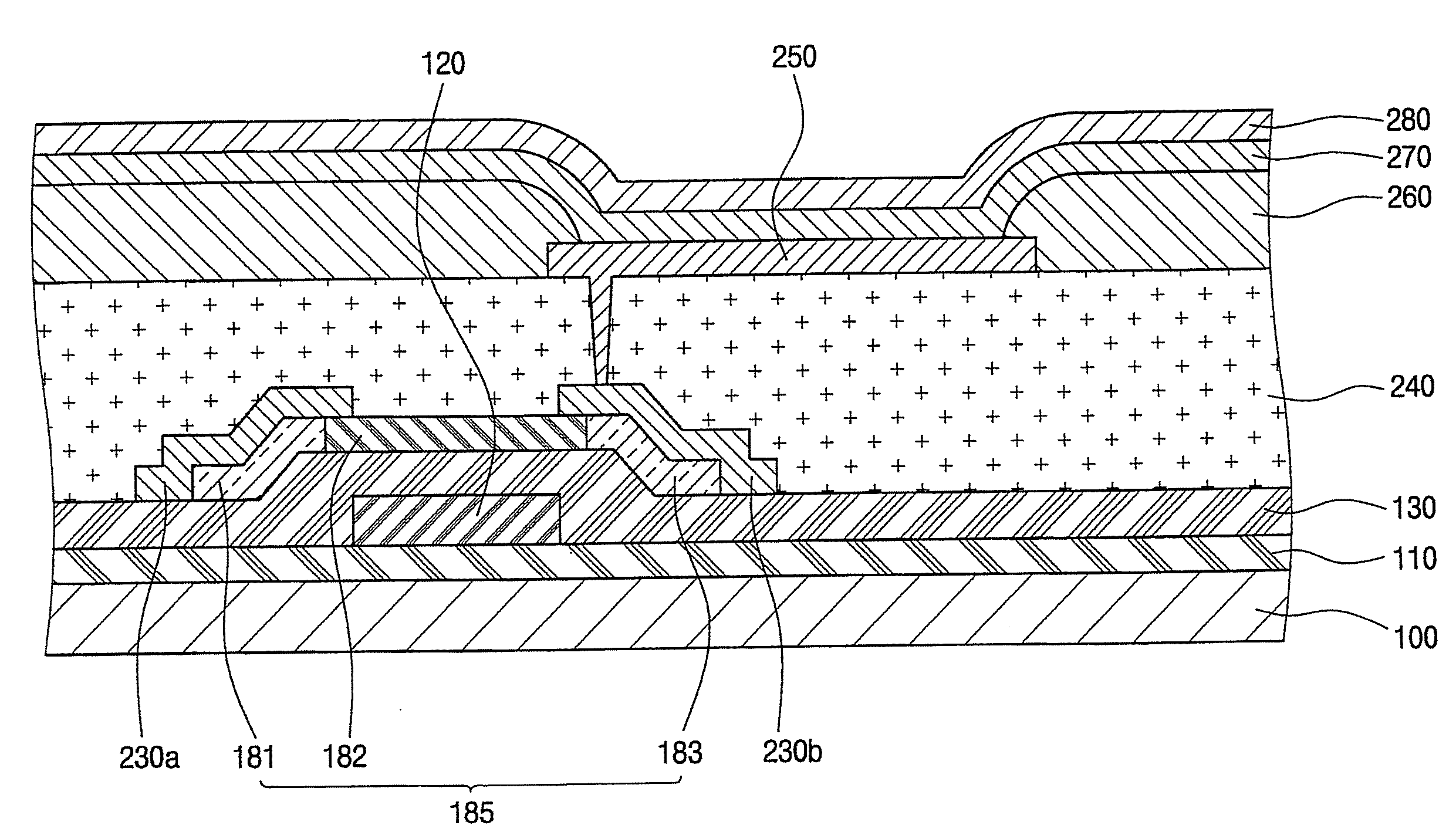
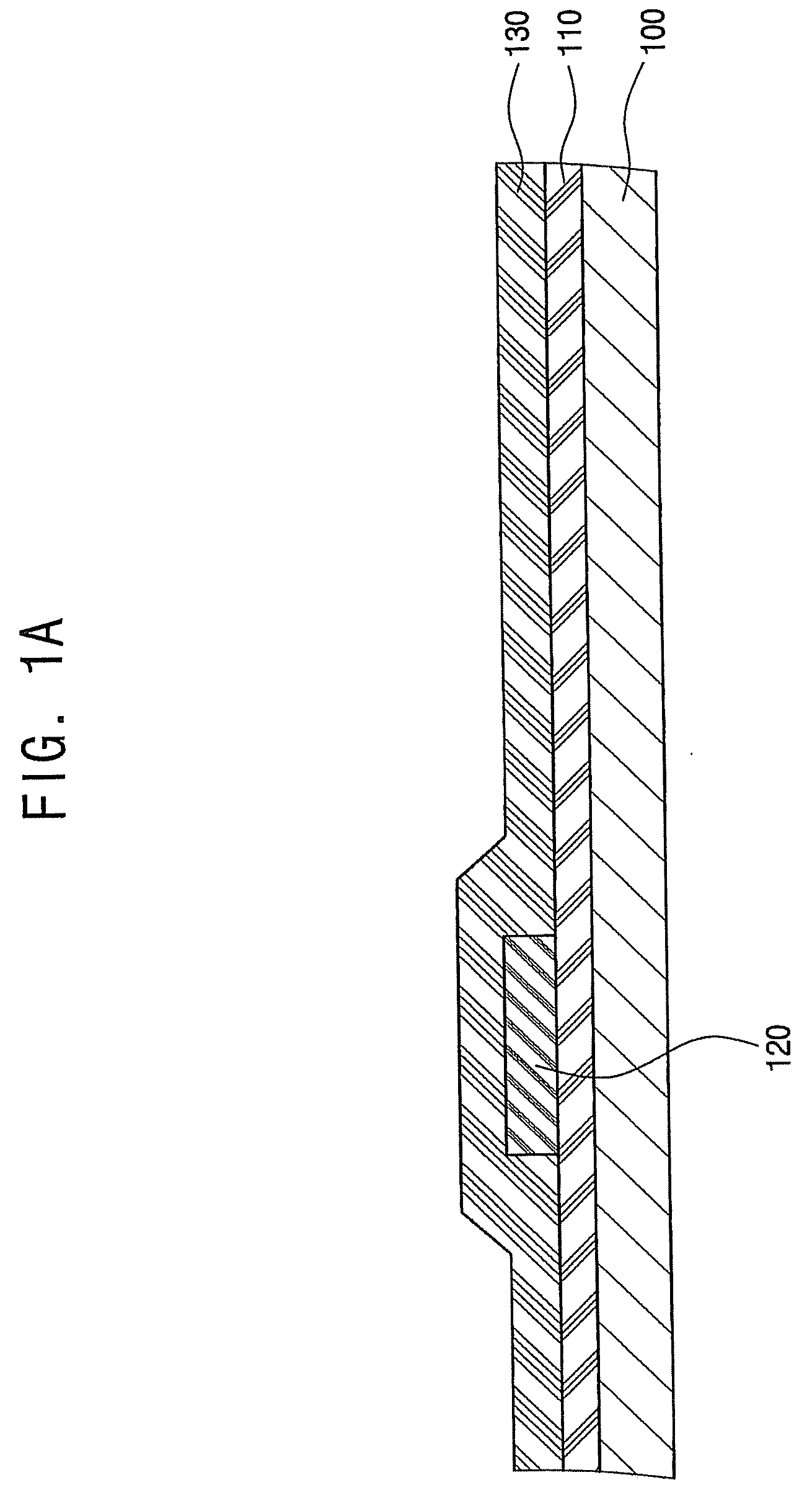
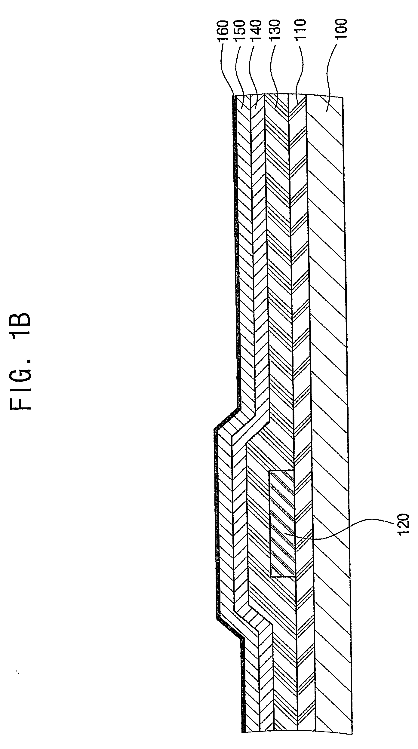
[0019]Reference will now be made in detail to the exemplary embodiments of the present invention, examples of which are illustrated in the accompanying drawings, wherein like reference numerals refer to the like elements throughout. The exemplary embodiments are described below, in order to explain the aspects of the present invention, by referring to the figures. As referred to herein, when a first element is said to be disposed or formed “on”, or “adjacent to”, a second element, the first element can directly contact the second element, or can be separated from the second element by one or more other elements located therebetween. In contrast, when an element is referred to as being disposed or formed “directly on” another element, there are no intervening elements present. As used herein, the term “and / or” includes any and all combinations of one or more of the associated listed items.

[0020]FIGS. 1A through 1D are cross-sectional views illustrating a crystallization process, acco...


PUM


Abstract

A thin film transistor (TFT), a method of fabricating the same, and an organic light emitting diode (OLED) display device having the TFT, the TFT including a substrate, a gate electrode disposed on the substrate, a gate insulating layer disposed on the gate electrode, a semiconductor layer disposed on the gate insulating layer and crystallized using a metal catalyst, and source and drain electrodes disposed on the semiconductor layer and electrically connected to source and drain regions of the semiconductor layer. A second metal is diffused into a surface region of the semiconductor layer, to getter the metal catalyst from a channel region of the semiconductor layer. The second metal can have a lower diffusion coefficient in silicon than the metal catalyst.

Description

CROSS-REFERENCE TO RELATED APPLICATIONS[0001]This application claims the benefit of Korean Patent Application No. 2008-8159, filed Jan. 25, 2008, the disclosure of which is hereby incorporated herein by reference in its entirety.BACKGROUND OF THE INVENTION[0002]1. Field of the Invention[0003]Aspects of the present invention relate to a thin film transistor (TFT), a method of fabricating the same, and an organic light emitting diode (OLED) display device having the TFT.[0004]2. Description of the Related Art[0005]In general, a polycrystalline silicon (poly-Si) layer is widely used as a semiconductor layer of a thin film transistor (TFT), because the poly-Si layer has a high field-effect mobility, can be applied to a high-speed operating circuit, and can be used to configure a complementary-metal-oxide-semiconductor (CMOS) circuit. A TFT including the poly-Si layer is typically used as an active device of an active-matrix liquid crystal display (AMLCD), or a switching or driving devic...

Claims


Application Information

Patent Timeline
Patent Type & Authority Applications(United States)
IPC IPC(8): H01L33/00H01L21/84H01J1/62H01L21/20H01L21/336H01L29/786
CPCH01L21/02488H01L21/02532H01L27/1277H01L29/458H01L29/66765H01L21/02672H01L27/1214
Inventor AHN, JI-SUPARK, BYOUNG-KEONYANG, TAE-HOONSEO, JIN-WOOKLEE, KIL-WONLEE, KI-YONGKIM, SUNG-CHUL
Owner SAMSUNG DISPLAY CO LTD
Why Eureka
Try Eureka