Semiconductor device and manufacturing method of the same

a technology of semiconductor devices and semiconductors, applied in semiconductor devices, diodes, electrical apparatuses, etc., can solve the problems of limiting the reduction of resistance, and achieve the effect of large power

Active Publication Date: 2009-07-30
RENESAS ELECTRONICS CORP
View PDF3 Cites 57 Cited by
  • Summary
  • Abstract
  • Description
  • Claims
  • Application Information

AI Technical Summary

Benefits of technology

[0007]A planar type power MISFET has generally been used for the power MISFET. The planar type power MISFET is one that takes a structure in which a gate electrode is formed over a main surface of a semiconductor substrate. Since it is however difficult to reduce a cell size in the planar type power MISFET, there was a limit to a reduction in on resistance. Thus, examinations for adopting a trench type power MISFET in place of the planar type power MISFET thereby to shrink each cell and reducing on resistance as compared with the planar type power MISFET have been conducted.
[0026]A trench gate type power MISFET equipped with a current detection circuit is capable of achieving an improvement in current detection accuracy.

Problems solved by technology

Since it is however difficult to reduce a cell size in the planar type power MISFET, there was a limit to a reduction in on resistance.

Method used


Image

  • Semiconductor device and manufacturing method of the same
  • Semiconductor device and manufacturing method of the same
  • Semiconductor device and manufacturing method of the same

Examples


first embodiment

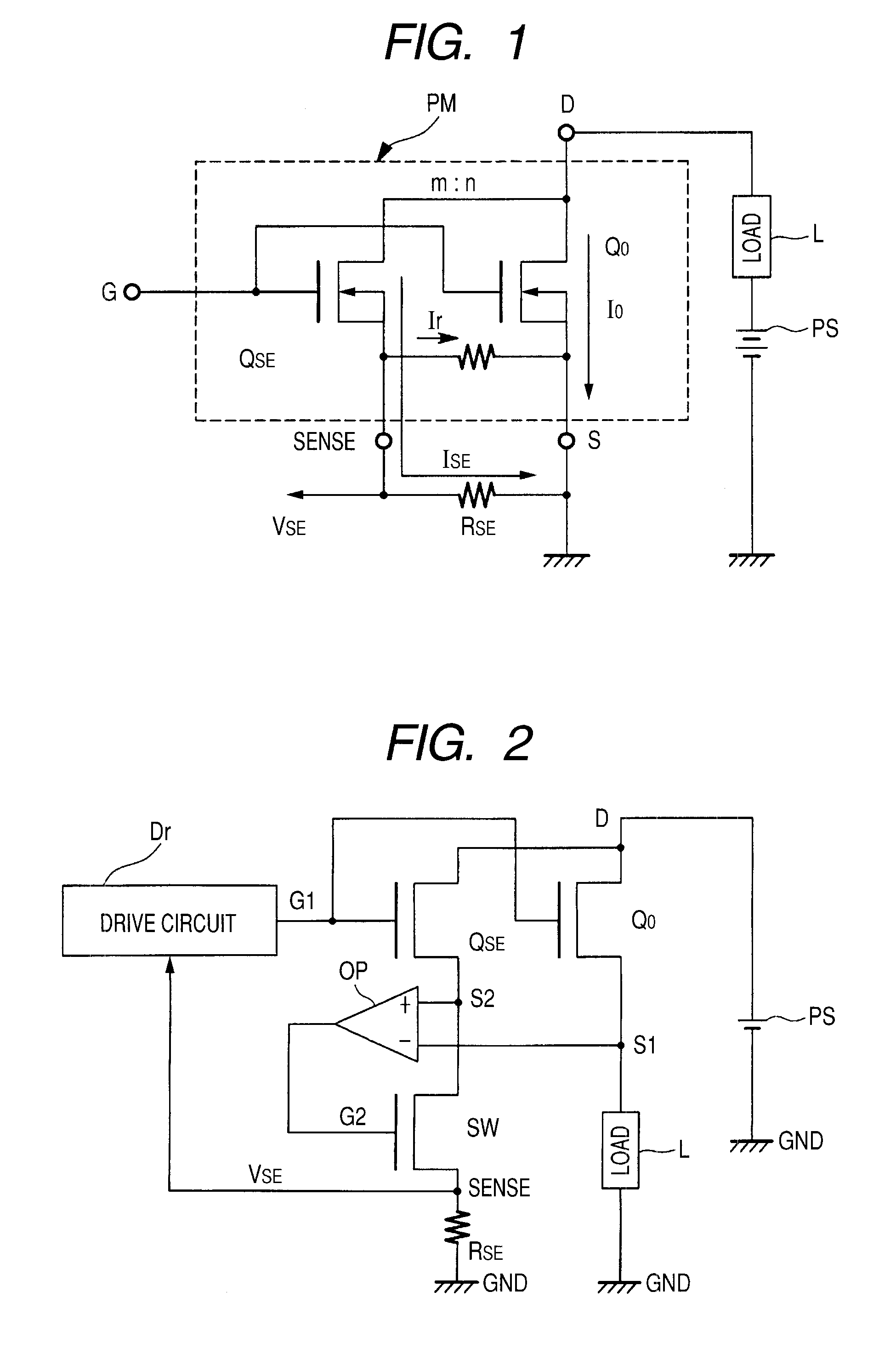
[0076]When overcurrent of a rated value or more flows in a semiconductor device using a power MISFET, there is a fear that a load circuit (element) coupled to the power MISFET or the power MISFET itself (element) is destroyed. Therefore, the semiconductor device using the power MISFET is provided with a function for preventing the breakdown of each element due to the overcurrent. An example of a circuit for preventing the breakdown of each element due to the overcurrent will be explained.

[0077]FIG. 2 is a circuit diagram showing a circuit for driving a load using a power MISFET having a current sensing or detection circuit. In FIG. 2, a drain terminal D of a main cell (power MISFET) Q0 is coupled to a power supply PS. A load L is coupled between a source terminal S1 of the main cell Q0 and GND. The drain terminal D of the main cell Q0 is used in common with a drain terminal D of a sense cell (power MISFET) QSE. Further, a gate terminal G1 of the main cell Q0 and a gate terminal G1 o...

second embodiment

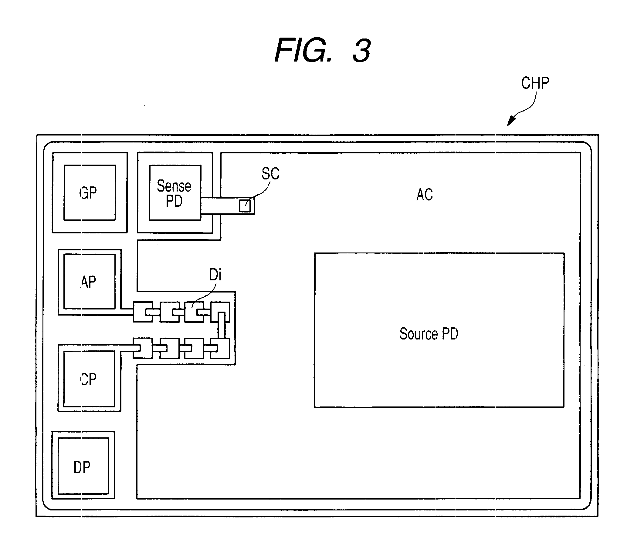
[0137]The present embodiment will explain a configuration of a power MISFET capable of enhancing a breakdown voltage (BVdss) in addition to the configuration of the first embodiment. FIG. 16 is a plan view showing part of the power MISFET according to the second embodiment. FIG. 16 shows an active cell AC corresponding to the power MISFET, a sense cell SC for current detection, and inactive cells IAC provided around a sense cell SC to separate the active cell AC and the sense cell SC from each other. This configuration is similar to the first embodiment. The active cell AC, the sense cell SC and the inactive cells IAC comprise a trench gate type power MISFET. Here, the power MISFET according to the second embodiment differs from the power MISFET according to the first embodiment in that an electric field relaxation layer 18 is provided in a peripheral area or region that surrounds the sense cell SC. The electric field relaxation layer 18 comprises a p-type semiconductor region.

[0138...

third embodiment

[0141]Although the first embodiment has explained the configuration in which the leak current developed between the sense cell SC and the active cell AC is reduced, the present embodiment will also explain an example of another configuration in which a leak current developed between a sense cell SC and an active cell AC can be reduced, and a configuration example capable of realizing a further reduction in the leak current.

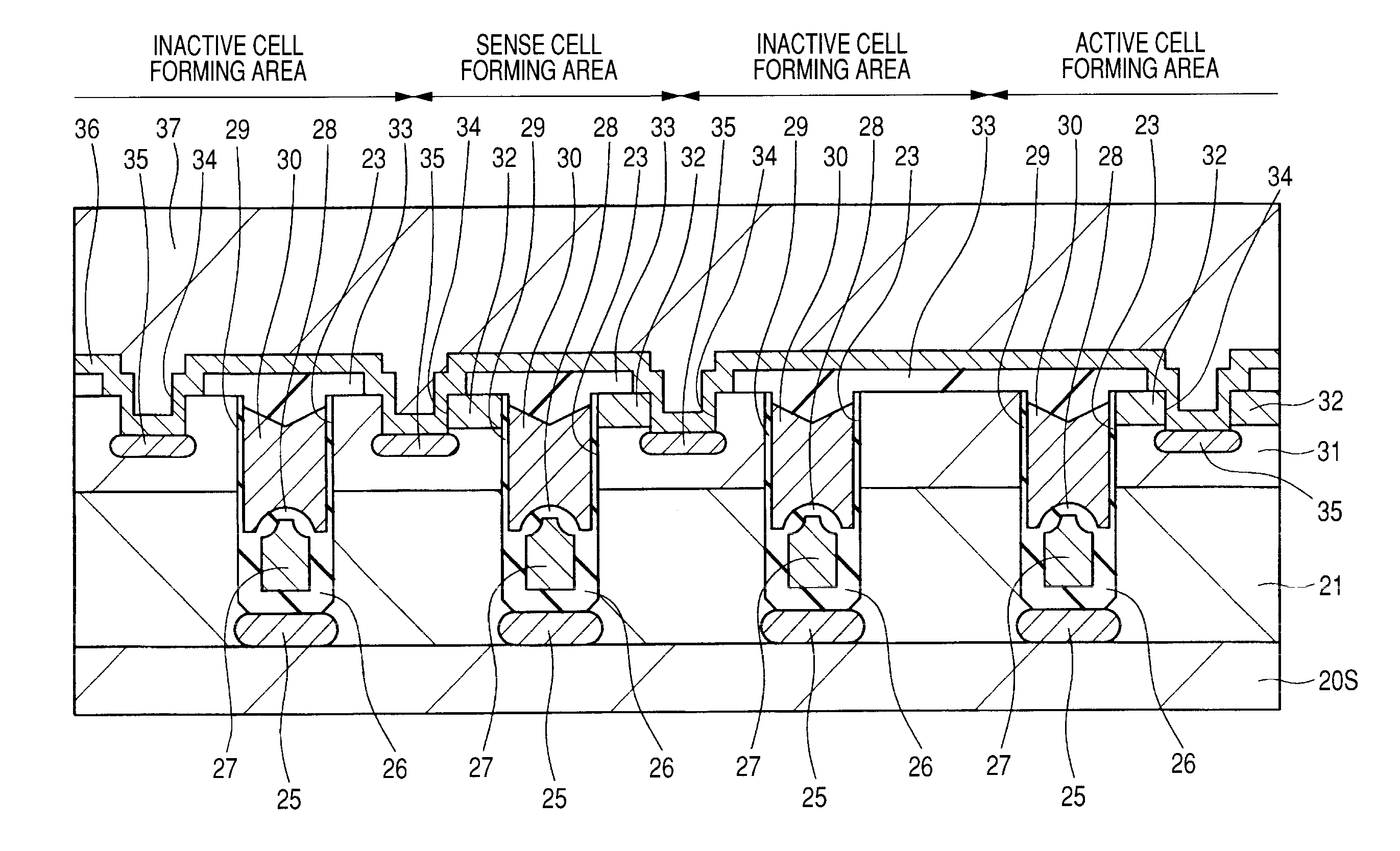
[0142]FIG. 18 is a sectional view showing a structure in which a leak current developed between a sense cell SC and an active cell AC presents a problem. The sense cell SC, active cell AC and inactive cells IAC are illustrated in FIG. 18. A description will first be made of a configuration of a sense cell SC formed in its corresponding sense cell forming area. In FIG. 18, an n-type epitaxial layer 21 in which an n-type impurity such as phosphorus or arsenic has been introduced, is formed over a semiconductor substrate 20S. A channel forming region (semiconductor r...


PUM


Abstract

The present invention provides a technique capable of attaining an improvement in current detection accuracy in a trench gate type power MISFET equipped with a current detection circuit. Inactive cells are disposed so as to surround the periphery of a sense cell. That is, the inactive cell is provided between the sense cell and an active cell. All of the sense cell, active cell and inactive cells are respectively formed of a trench gate type power MISFET equipped with a dummy gate electrode. At this time, the depth of each trench extends through a channel forming region and is formed up to the deep inside (the neighborhood of a boundary with a semiconductor substrate) of an n-type epitaxial layer. Further, a p-type semiconductor region is provided at a lower portion of each trench. The p-type semiconductor region is formed so as to contact the semiconductor substrate.

Description

CROSS-REFERENCE TO RELATED APPLICATIONS[0001]The disclosure of Japanese Patent Application No. 2008-19156 filed on Jan. 30, 2008 including the specification, drawings and abstract is incorporated herein by reference in its entirety.BACKGROUND OF THE INVENTION[0002]The present invention relates to a semiconductor device and its manufacturing technology, and particularly to a technique effective if applied to a semiconductor device having a power MISFET (Metal Insulator Semiconductor Field Effect Transistor).[0003]A technique for causing a sense cell to divert a load current flowing through a power MISFET and detecting the load current flowing through the power MISFET by utilizing a voltage drop developed across a sense resistor coupled to the sense cell has been described in Japanese Unexamined Patent Publication No. He 3(1991)-270274 (patent document 1). Described specifically, since an insulating film of a portion interposed between a gate insulating film of a power MISFET (main un...

Claims


Application Information

Patent Timeline
Patent Type & Authority Applications(United States)
IPC IPC(8): H01L29/78H01L21/336
CPCH01L29/0619H01L27/088H01L29/0646H01L29/0696H01L29/407H01L29/41766H01L29/4236H01L29/42368H01L29/42376H01L29/4238H01L29/66727H01L29/66734H01L29/7804H01L29/7813H01L29/7815H01L29/0623H01L2224/48247H01L2224/05554H01L2224/0603H01L2224/48137H01L2224/49111H01L2924/13091H01L2224/02166H01L2924/00
Inventor SHINBORI, ATSUSHINAKAZAWA, YOSHITO
Owner RENESAS ELECTRONICS CORP
Why Eureka
Try Eureka