Semiconductor device

a technology of semiconductor devices and carriers, applied in semiconductor devices, diodes, electrical apparatus, etc., can solve the problems that carriers based on counter-electromotive force injected from output elements cannot reach the other element formation region without bypassing, and increase the possibility of carriers disappearing in the course due to recombination, so as to achieve high-efficiency preventing the movement of electrons and reducing the size of chips

Active Publication Date: 2009-07-30
RENESAS ELECTRONICS CORP
View PDF2 Cites 14 Cited by
  • Summary
  • Abstract
  • Description
  • Claims
  • Application Information

AI Technical Summary

Benefits of technology

[0009]The present invention is made in view of the aforementioned problem, and the object of the present invention is to provide a semiconductor device which allows the chip size to be reduced easily and is highly effective in preventing movement of electrons from an output transistor formation region to an other element formation region.
[0011]In accordance with the semiconductor device in the present embodiment, a trench isolation structure is formed at least either between the active barrier region and the output element formation region or between the active barrier region and the other element formation region. Because of isolation by a trench in this manner, the two-dimensional area occupied by the isolation structure can be made smaller than the isolation using a pn junction. Therefore, the chip size can easily be reduced.
[0012]Furthermore, the trench is formed to extend from the main surface of the semiconductor substrate through the second region to reach the first region. Thus, carriers based on counter-electromotive force injected from the output element cannot reach the other element formation region without bypassing the trench. Accordingly, the movement path of carriers from the output element formation region to the other element formation region becomes longer, thereby increasing the possibility that the carriers disappear in the course due to recombination. Therefore, the movement of carriers based on counter-electromotive force from the output element formation region to the other element formation region can be inhibited, thereby preventing a malfunction of the other elements.

Problems solved by technology

Thus, carriers based on counter-electromotive force injected from the output element cannot reach the other element formation region without bypassing the trench.
Accordingly, the movement path of carriers from the output element formation region to the other element formation region becomes longer, thereby increasing the possibility that the carriers disappear in the course due to recombination.

Method used


Image

  • Semiconductor device
  • Semiconductor device
  • Semiconductor device

Examples


first embodiment

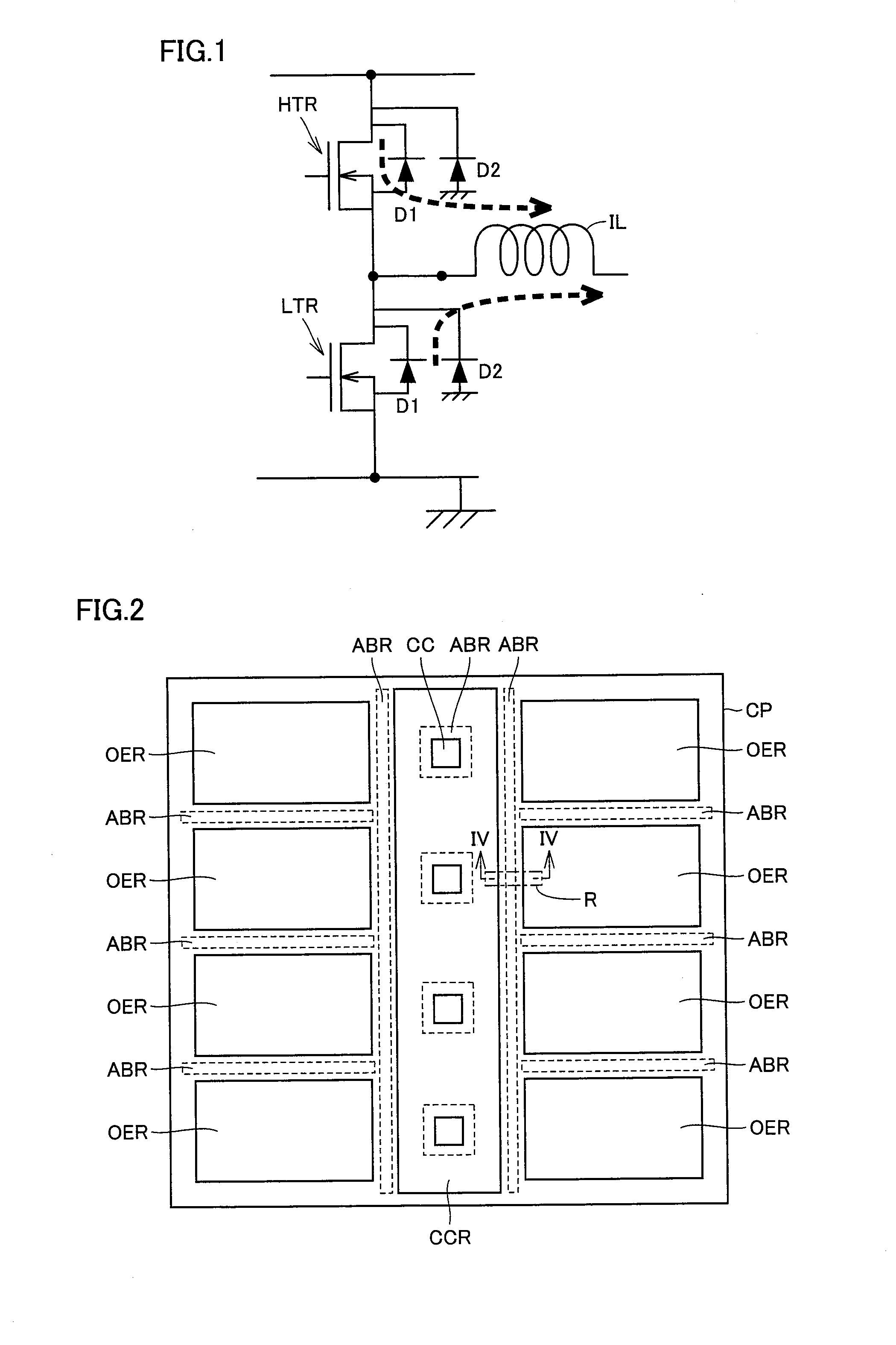
[0035]Referring to FIG. 1, an output element formed in a semiconductor chip includes, for example, a high-voltage High side n-channel MOS (Metal Oxide Semiconductor) transistor (referred to as an nMOS transistor hereinafter) HTR and a high-voltage Low side nMOS transistor LTR.

[0036]A diode D1 is formed between the back gate and the drain of each of nMOS transistor HTR and nMOS transistor LTR. In addition, a diode D2 is formed between a p-type semiconductor substrate and the drain of each of nMOS transistor HTR and nMOS transistor LTR.

[0037]The source of nMOS transistor HTR and the drain of nMOS transistor LTR are electrically connected to each other and are electrically connected to an inductive load (for example, a coil) IL arranged on the outside of the semiconductor chip.

[0038]It is noted that an output element refers to an element electrically connected to an electronic device arranged on the outside of a semiconductor chip.

[0039]Referring to FIG. 2, a semiconductor chip CP has,...

second embodiment

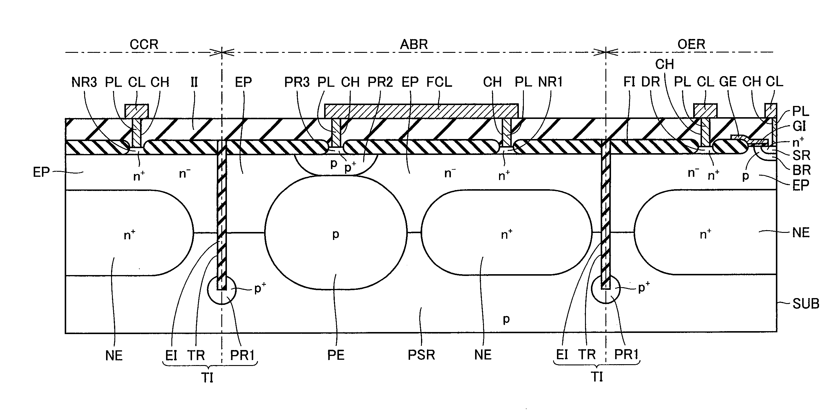
[0102]Referring to FIG. 14, the configuration of the present embodiment differs from the configuration of the first embodiment shown in FIG. 4 in that a trench structure is added.

[0103]In the present embodiment, trench TR is formed to extend from the main surface of semiconductor substrate SUB to between buried p-type diffusion region PE and buried n+ diffusion region NE in active barrier region ABR. Buried insulating layer EI is formed in trench TR. In addition, p+ diffusion region PR1 is formed to surround the lower end part of trench TR.

[0104]This trench TR passes through n− epitaxial layer EP to reach p-type impurity region PSR. Furthermore, this trench TR preferably extends to a position deeper than the lowermost part of buried p-type diffusion region PE and buried n+ diffusion region NE relative to the main surface of semiconductor substrate SUB.

[0105]Here, the other configuration of the structure of the present embodiment is almost the same with the configuration of the foreg...

third embodiment

[0109]Referring to FIG. 17, the configuration of the present embodiment differs from the configuration of the first embodiment shown in FIG. 4 in that the p-type diffusion region and the n-type diffusion region that form the active barrier structure are reversely arranged.

[0110]In the present embodiment, the p-type diffusion region (buried p-type diffusion region PE, p-type diffusion region PR2, p+ diffusion region PR3) that forms the active barrier structure is positioned on the output transistor formation region OER side while the n-type diffusion region (buried n+ diffusion region NE, n+ diffusion region NR1) is positioned on the control circuit formation region CCR side.

[0111]Here, the other configuration of the structure of the present embodiment is almost the same with the configuration of the foregoing first embodiment, and therefore the same components are denoted with the same characters and the description thereof will not be repeated.

[0112]Referring to FIG. 18, even when ...


PUM


Abstract

An active barrier structure has a p-type region and an n-type region, each of which is in contact with a p-type impurity region and which are ohmic-connected to each other to attain a floating potential. A trench isolation structure is formed between an active barrier region and the other region (an output transistor formation region and a control circuit formation region). The trench isolation structure has a trench extending from the main surface of the semiconductor substrate through the n− epitaxial layer to reach the p-type impurity region. Therefore, a semiconductor device is obtained which allows the chip size to be reduced easily and is highly effective in preventing movement of electrons from the output transistor formation region to the other element formation region.

Description

BACKGROUND OF THE INVENTION[0001]1. Field of the Invention[0002]The present invention relates to a semiconductor device, and more particularly to a semiconductor device having an output element formation region, an other element formation region, and an active barrier region arranged between the output element formation region and the other element formation region.[0003]2. Description of the Background Art[0004]In products used for automobiles, motor drive, audio amplifiers, and the like, an L (self inductance) load sometimes produces counter-electromotive force to cause the drain (n-type region) of an output transistor to have a negative potential. In this case, the negative potential allows electrons to be injected from the drain to a p-type substrate and move from an output transistor formation region to an other element formation region through the p-type substrate, causing the other elements to malfunction. To solve this problem, an active barrier region may be formed between ...

Claims


Application Information

Patent Timeline
Patent Type & Authority Applications(United States)
IPC IPC(8): H01L29/06
CPCH01L27/0629H01L27/088H01L29/7816H01L29/42368H01L29/0878
Inventor YAMAMOTO, FUMITOSHI
Owner RENESAS ELECTRONICS CORP
Why Eureka
Try Eureka