Solid-state image pickup element and solid-state image pickup device

a pickup device and solid-state image technology, applied in the direction of radio frequency controlled devices, television system scanning details, television systems, etc., can solve the problems of reducing the size of the pixel, and forming the remarkable silicon substrate as the thin film becomes thin, so as to achieve uniform and accurate discharging of excessive charges

Active Publication Date: 2009-07-30
KK TOSHIBA
View PDF2 Cites 26 Cited by
  • Summary
  • Abstract
  • Description
  • Claims
  • Application Information

AI Technical Summary

Benefits of technology

[0016]The present invention has been made in view of these circumstances, and an object thereof is to provide a solid-state image pickup element and a solid-state image pickup device capable of uniformly and accurately discharging excessive charges generated when high light is incident.

Problems solved by technology

It has become an important issue to make the pixel size smaller.
Problems caused by this are being actualized.
A problem posed by the silicon substrate formed as the thin film becomes remarkable when the incident light intensity is high, i.e., when an image of high light is taken.
In other words, if excessive electron-hole pairs are generated by incidence of the high light, then excessive signal electrons which have exceeded the saturation charge quantity of the photodiode overflow and are injected into a photodiode of an adjacent pixel, resulting in a problem of blooming or crosstalk.
In this method, however, the barrier height of the overflow channel is controlled by using a silicon substrate impurity concentration which is an extremely low concentration, and consequently its control is substantially difficult.

Method used


Image

  • Solid-state image pickup element and solid-state image pickup device
  • Solid-state image pickup element and solid-state image pickup device
  • Solid-state image pickup element and solid-state image pickup device

Examples


Embodiment Construction

[0023]Hereafter, embodiments of the present invention will be described in detail with reference to the drawings. In the drawings, the same parts are denoted by like reference characters and duplicated description will not be repeated. Furthermore, the drawings are schematic, and relations between thickness and plane dimensions and ratios between thicknesses of layers are different from actual values.

[0024]In addition, parts which are different in mutual relations between dimensions and ratios are included between drawings as well.

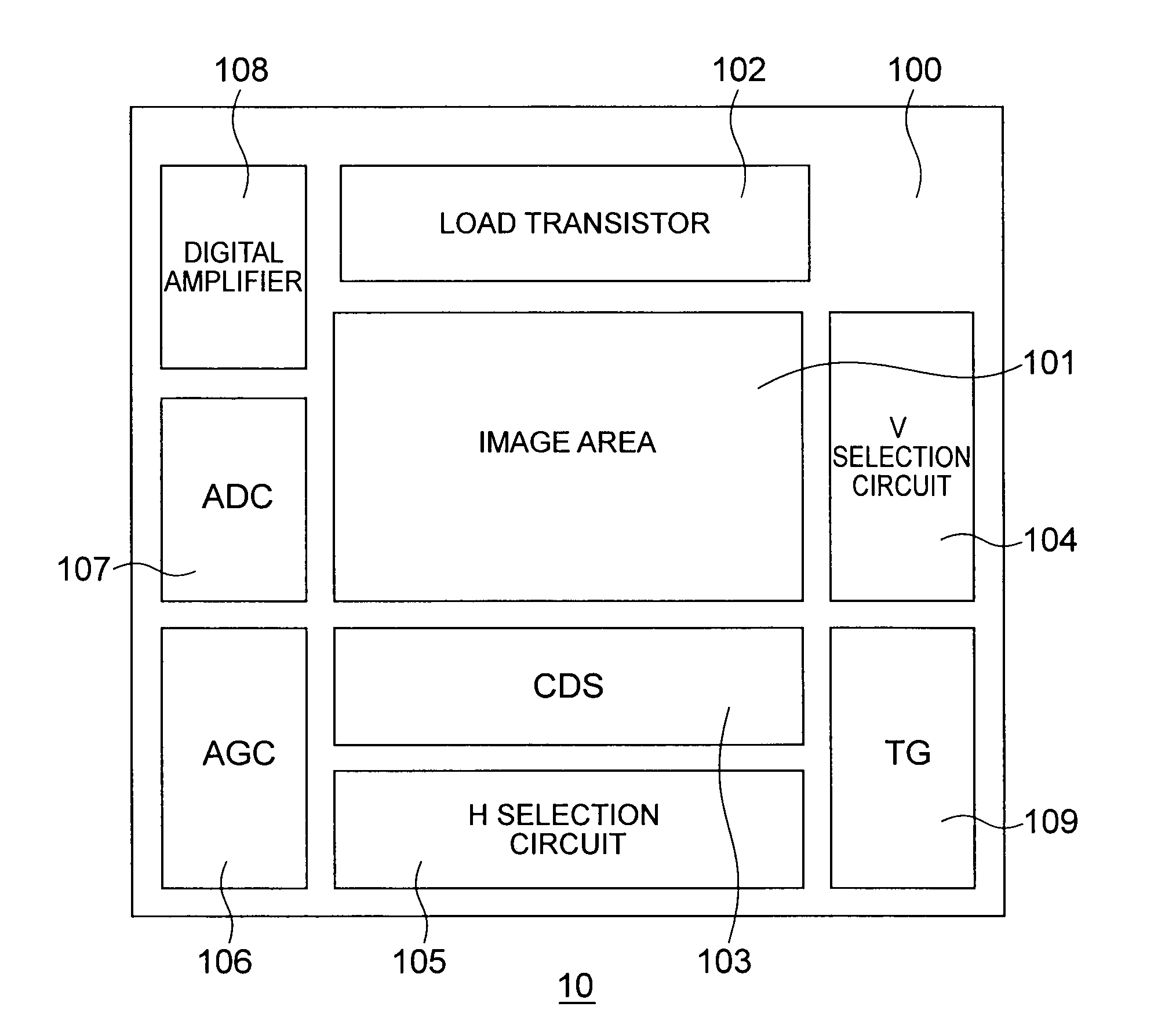
[0025]A solid-state image pickup element according to an embodiment of the present invention is shown in FIG. 1. A solid-state image pickup element 10 according to the present embodiment is formed on a solid-state image pickup element chip 100.

[0026]The solid-state image pickup element chip 100 includes an image area 101 having photoelectric conversion pixels arranged as a two-dimensional array to convert an incident optical signal to an electric signal by...


PUM


Abstract

A solid-state image pickup element includes: a semiconductor layer of a first conductivity type; a pixel area having pixels formed in a matrix form, each of the pixels including a photoelectric conversion element having a pn junction formed of the semiconductor layer of the first conductivity type and a first semiconductor region of a second conductivity type, a second semiconductor region of the first conductivity type formed on a first surface side of the semiconductor layer, and potential control wiring connected electrically to the second semiconductor region; and a pixel signal readout circuit including at least one MOS transistor formed on the first surface side of the semiconductor layer in the pixel area to have a source and a drain formed of an impurity region of the second conductivity type. Incidence of light to the photoelectric conversion element is made from a second surface side opposite to the first surface side.

Description

CROSS-REFERENCE TO RELATED APPLICATION[0001]This application is based upon and claims the benefit of priority from prior Japanese Patent Application No. 2008-17232 filed on Jan. 29, 2008 in Japan, the entire contents of which are incorporated herein by reference.BACKGROUND OF THE INVENTION[0002]1. Field of the Invention[0003]The present invention relates to a solid-state image pickup element and a solid-state image pickup device.[0004]2. Related Art[0005]Because of spread of the digital camera and the cellular phone with built-in camera in recent years, demands for the solid-state image pickup element are increasing. In particular, demands for the CMOS solid-state image pickup element which can be manufactured by the CMOS process which is a general semiconductor manufacturing process arise. In recent years, such a solid-state image pickup element is required to have a smaller size and a larger number of pixels. It has become an important issue to make the pixel size smaller.[0006]As...

Claims


Application Information

Patent Timeline
Patent Type & Authority Applications(United States)
IPC IPC(8): H04N5/335H01L27/146H04N5/359H04N5/369H04N5/374H04N5/3745H04N5/376
CPCH01L27/1203H01L27/14623H01L27/14636H01L27/1464H04N5/3592H04N5/3741H04N5/3745H01L27/14656H04N25/622H04N25/766H04N25/77
Inventor IIDA, YOSHINORI
Owner KK TOSHIBA
Why Eureka
Try Eureka