
Silicon carbide semiconductor device including deep layer

a silicon carbide semiconductor and deep layer technology, applied in semiconductor devices, radiation control devices, electrical devices, etc., can solve the problems of gate insulating layer damage, further relaxation of electric field, and difficulty, and achieve the effect of increasing the breakdown voltage of the sic semiconductor devi

Active Publication Date: 2009-08-13
DENSO CORP
View PDF31 Cites 103 Cited by
  • Summary
  • Abstract
  • Description
  • Claims
  • Application Information

AI Technical Summary

Benefits of technology

[0013]In the present SiC semiconductor device, the deep layer is formed along a direction approximately perpendicular to a longitudinal direction of the trench. Thus, a misalignment of a mask for forming the trench and a mask for forming the deep layer does not affect a property of the SiC semiconductor device. Thereby, a variation of a production property can be reduced and a yield can be improved.
[0015]In the present SiC semiconductor device, the deep layer is formed along a direction approximately perpendicular to a longitudinal direction of the trench. Thus, a misalignment of a mask for forming the trench and a mask for forming the deep layer does not affect a property of the SiC semiconductor device. Thereby, a variation of a production property can be reduced and a yield can be improved.
[0017]In the present SiC semiconductor device, an on-resistance can be reduced and a breakdown voltage can be increased due to the body layer having the impurity concentration greater than the impurity concentration of the base region.
[0019]In the present SiC semiconductor device, a portion where a breakdown can possibly occur is moved to the peripheral section due to the outer edge portion of the deep layer located at the outer edge portion of the cell section. Thus, a breakdown voltage of the SiC semiconductor device can be increased.
[0021]In the present SiC semiconductor device, a portion where a breakdown can possibly occur is moved to the peripheral section due to the outer edge portion of the deep layer located at the outer edge portion of the cell section. Thus, a breakdown voltage of the SiC semiconductor device can be increased.

Problems solved by technology

When a trench gate structure is applied to the SiC semiconductor device, difficulty arises.
As a result, the gate insulating layer may be damaged, for example, at a corner portion of each of the trenches.
However, further relaxation of the electric field is required.
Thus, a positioning is difficult, and a distance between a sidewall of the trench and the P type deep layer may vary.

Method used


Image

  • Silicon carbide semiconductor device including deep layer
  • Silicon carbide semiconductor device including deep layer
  • Silicon carbide semiconductor device including deep layer

Examples


first embodiment

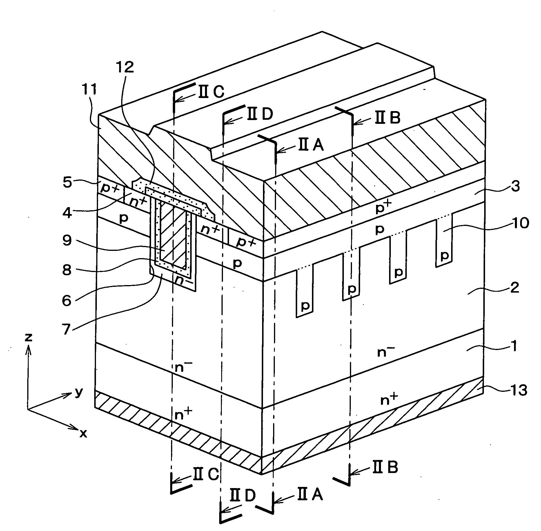
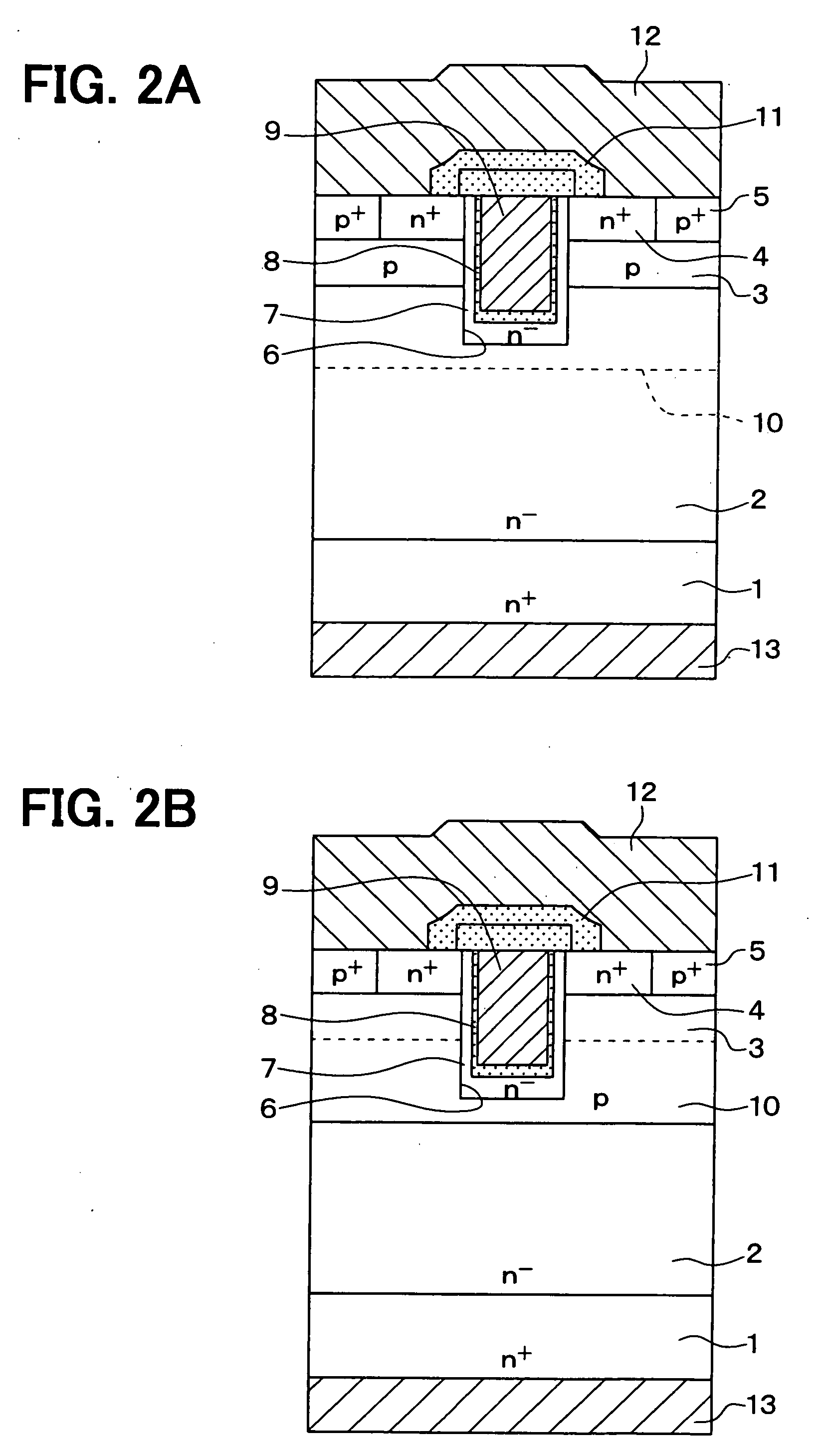
[0090]An SiC semiconductor device according to a first embodiment of the present invention will now be described with reference to FIG. 1 to FIG. 2D. The SiC semiconductor device includes a plurality of accumulation type MOSFETs, for example.

[0091]One of the MOSFETs is illustrated in FIG. 1. In the SiC semiconductor device, the MOSFETs are arranged in a plurality of rows so as to be adjacent to each other.

[0092]The MOSFET includes an N+ type substrate 1 made of SiC. The N+ type substrate 1 includes, for example, phosphorus as N type impurities. An impurity concentration of the N+ type substrate 1 is, for example, about 1.0×1019 cm−3. The N+ type substrate 1 has a thickness of, for example, about 300 μm. On a front surface of the N+ type substrate 1, an N− type drift layer 2 made of SiC is located. The N− type drift layer 2 includes, for example, phosphorus as N type impurities. An impurity concentration of the N− type drift layer 2 is, for example, between about 3.0×1015 cm−3 and ab...

second embodiment

[0120]An SiC semiconductor device according to a second embodiment of the present invention will be described with reference to FIG. 7 to FIG. 8D. As illustrated in FIG. 7, in a MOSFET included in the SiC semiconductor device according to the present embodiment, an N type current diffusion layer 30 is disposed between the N− type drift layer 2 and the P type base region 3 so as to be in contact with the N type channel layer 7. The N type current diffusion layer 30 includes, for example, phosphorous as N type impurities. A concentration of the N type impurities in the N type current diffusion layer 30 is set to be greater than the concentration of the N type impurity in the N− type drift layer 2. The concentration of the N type impurity in the N type current diffusion layer 30 may be greater than the concentration of the N type impurity in the N type channel layer 7. For example, the impurity concentration in the N type current diffusion layer 30 is between about 2.0×1015 cm−3 and ab...

third embodiment

[0123]An SiC semiconductor device according to a third embodiment of the present invention will be described with reference to FIG. 11 to FIG. 12D.

[0124]As illustrated in FIG. 11, in a MOSFET included in the SiC semiconductor device according to the present embodiment, the N type current diffusion layer 30 is disposed between the N− type drift layer 2 and the P type base region 3 so as to be in contact with the N type channel layer 7. The P type deep layers 10 extend from the front surface of the N type current diffusion layer 30. The P type deep layers 10 penetrate through the N type current diffusion layer 30 and are contact with the P type base region 3. For example, the P type deep layers 10 have a depth between about 0.6 μm and about 1.0 μm from the front surface of the N type current diffusion layer 30. An impurity concentration, a width, and an interval of the P type deep layers 10 according to the present embodiment are similar to those of the P type deep layers 10 illustrat...


PUM


Abstract

A silicon carbide semiconductor device includes a substrate, a drift layer located on a first surface of the substrate, a base region located on the drift layer, a source region located on the base region, a trench penetrating the source region and the base region to the drift layer, a channel layer located in the trench, a gate insulating layer located on the channel layer, a gate electrode located on the gate insulating layer, a source electrode electrically coupled with the source region and the base region, a drain electrode located on a second surface of the substrate, and a deep layer. The deep layer is located under the base region, extends to a depth deeper than the trench and is formed along an approximately normal direction to a sidewall of the trench.

Description

CROSS REFERENCE TO RELATED APPLICATIONS[0001]The present application is based on and claims priority to Japanese Patent Applications No. 2008-31704 filed on Feb. 13, 2008, No. 2008-322426 filed on Dec. 18, 2008, and No. 2008-322233 filed on Dec. 18, 2008, the contents of which are incorporated in their entirety herein by reference.BACKGROUND OF THE INVENTION[0002]1. Field of the Invention[0003]The present invention relates to a silicon carbide semiconductor device including a deep layer.[0004]2. Description of the Related Art[0005]A silicon carbide (SiC) semiconductor device typically has a high breakdown field strength and can therefore control a high current. The SiC semiconductor device can be used for controlling a motor of a hybrid vehicle, for example.[0006]In order to increase electric current that flows in a semiconductor device, a channel density can be increased. In a silicon semiconductor device, a metal-oxide semiconductor field-effect transistor (MOSFET) having a trench...

Claims


Application Information

Patent Timeline
IPC IPC(8): H01L29/15
CPCH01L29/0615H01L29/0619H01L29/0623H01L29/0634H01L29/0638H01L29/0661H01L29/7828H01L29/0878H01L29/1095H01L29/1608H01L29/66068H01L29/7811H01L29/7813H01L29/0847H01L29/086H01L29/42312
Inventor SUZUKI, NAOHIROOKUNO, EIICHIMATSUKI, HIDEO
Owner DENSO CORP
Features
  • Generate Ideas
  • Intellectual Property
  • Life Sciences
  • Materials
  • Tech Scout
  • Unparalleled Data Quality
  • Higher Quality Content
  • 60% Fewer Hallucinations
Learn More