Semiconductor light-emitting device

a technology of semiconductors and light-emitting devices, applied in the field of semiconductor light-emitting elements, can solve problems such as improved output and efficiency, and achieve the effects of improving output and efficiency, improving light-emitting face uniformity, and inadequate resistance to large power inputs

Inactive Publication Date: 2009-08-13
DIEBOLD NIXDORF +1
View PDF3 Cites 42 Cited by
  • Summary
  • Abstract
  • Description
  • Claims
  • Application Information

AI Technical Summary

Benefits of technology

[0023]As described above, a conventional light-emitting diode structure cannot eliminate various possible damages in manufacturing process steps, and is, therefore, inadequately resistant to a large power input and inadequately insulative, resulting in difficulty in giving an LED with improved output and efficiency. Furthermore, there has been a need for improving uniformity of a light-emitting face.

Problems solved by technology

As described above, a conventional light-emitting diode structure cannot eliminate various possible damages in manufacturing process steps, and is, therefore, inadequately resistant to a large power input and inadequately insulative, resulting in difficulty in giving an LED with improved output and efficiency.

Method used


Image

  • Semiconductor light-emitting device
  • Semiconductor light-emitting device
  • Semiconductor light-emitting device

Examples


embodiment 1

of a Manufacturing Process

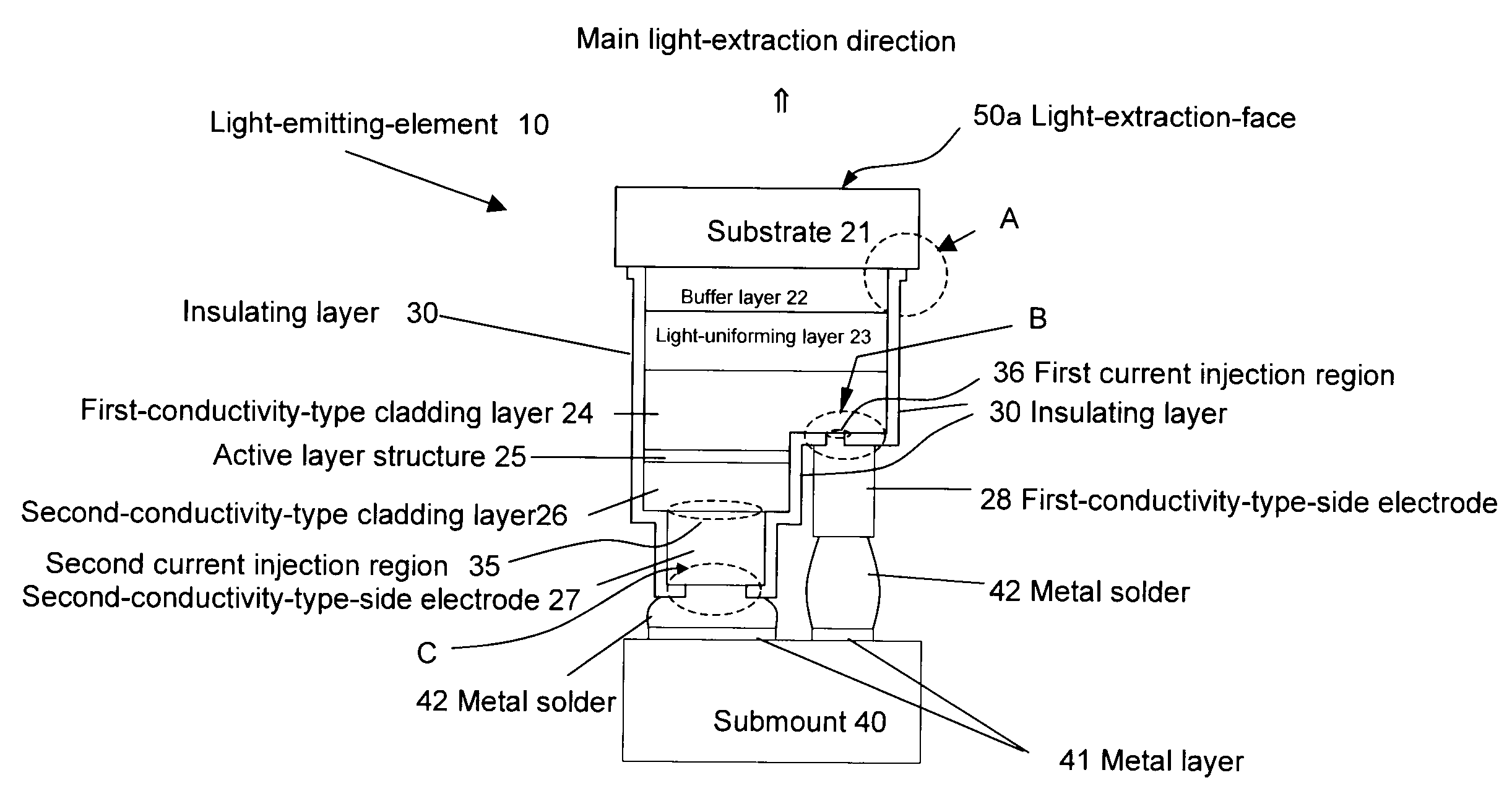
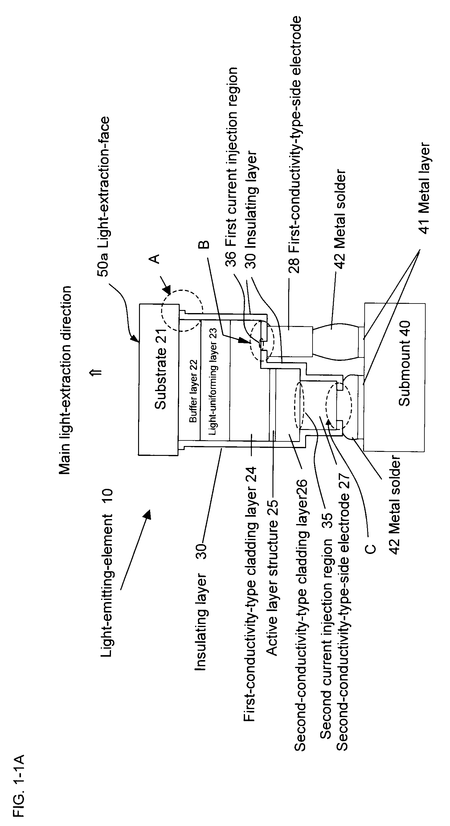
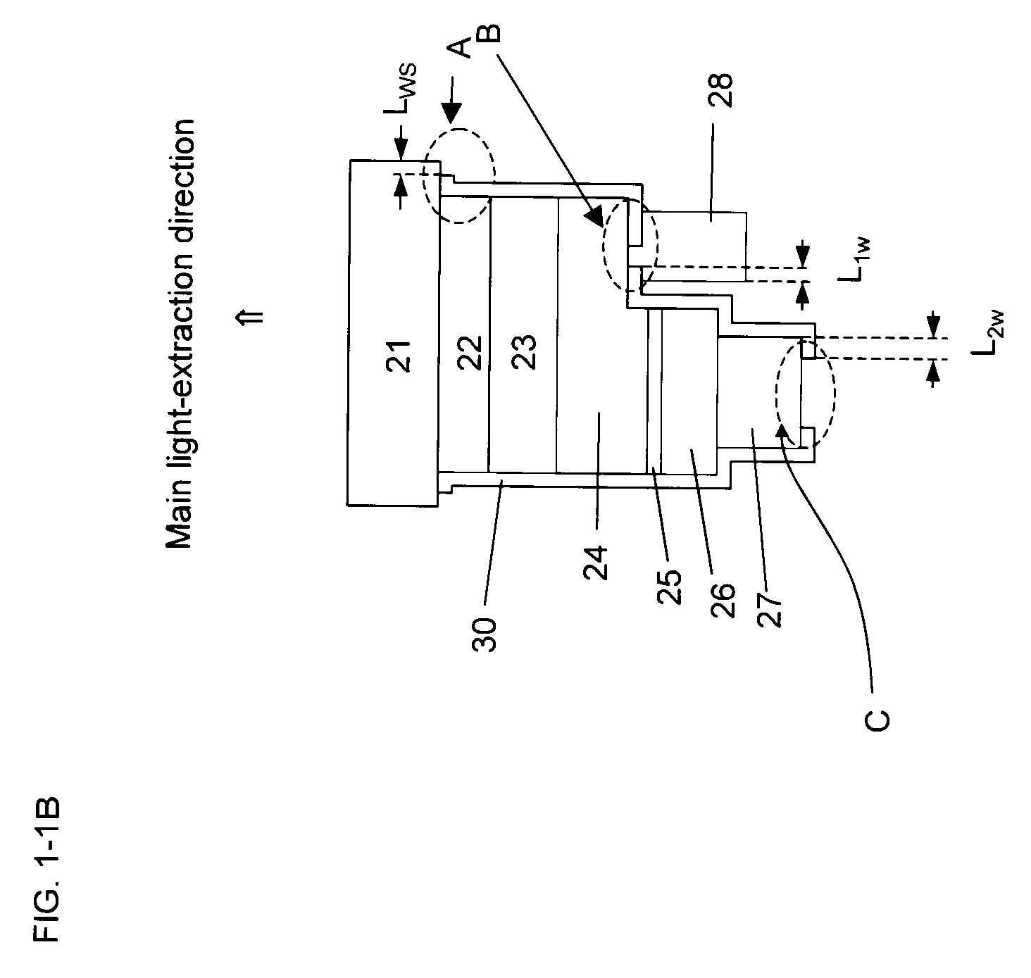
[0684]In Embodiment 1 of a manufacturing process, there will be described mainly a process for manufacturing a light-emitting-element shown in FIG. 4-1A and furthermore those for light-emitting-elements shown in FIG. 4-1C. As shown in FIG. 4-5, first a substrate 21 is provided and over the surface are sequentially deposited a buffer layer 22, a first-conductivity-type cladding layer 24, an active layer structure 25 and a second-conductivity-type cladding layer 26 by thin-film crystal growth. For formation of these thin-film crystal layers, MOCVD is preferably employed. However, it is possible to use MBE, PLD, PED, VPE and LPE processes for forming all or some of the thin-film crystal layers. A configuration of these layers can be appropriately changed, depending on, for example, an application of the element. After forming thin-film crystal layers, a variety of processings are allowed. As used herein, the term “thin-film crystal growth” includes heat-treatm...

embodiment 2

of a Manufacturing Process

[0723]In Embodiment 2 of a manufacturing process, there will be described mainly a process for manufacturing a light-emitting-element shown in FIG. 4-2A and furthermore those for light-emitting-elements shown in FIG. 4-2C. Embodiment 2 is conducted as described in Embodiment 1 until the step of forming an insulating layer 30 (FIG. 4-5 to FIG. 4-8). Then, in Embodiment 1, only a region including the center of a light-emitting-element separation-trench of the substrate surface (a trench bottom surface) while in Embodiment 2, as shown in FIG. 4-9B, all the insulating layer 30 over the substrate 21 (that is, the trench bottom surface) within the light-emitting-element separation-trench 13 is removed and the substrate-side (that is, the trench bottom surface side) insulating layer formed on the sidewall within the trench is removed to form a part without an insulating layer 15. The following process may be used as a formation process. First, a resist mask having...

examples

[0928]There will be described the present invention with reference to examples. Materials, amounts, proportions, specific processes and process orders in the following examples may be appropriately modified without departing from the scope of the invention. The scope of this invention should not be interpreted to be limited to the specific examples described below. Furthermore, in the drawings referred in the following examples, some sizes are deliberately changed to help understanding the structures, but practical dimensions are as indicated in the following description.

Examples of the Invention in Relation to Section A


PUM


Abstract

An etching process includes forming a metal-fluoride layer at least as a part of an etching mask formed over a semiconductor layer at a temperature of 150° C. or higher; patterning the metal-fluoride layer; and etching the semiconductor layer using the patterned metal-fluoride layer as a mask. Using this etching method, even an etching-resistant semiconductor layer such as a Group III-V nitride semiconductor can be easily etched by a relatively simpler process.

Description

TECHNICAL FIELD[0001]The present invention relates to a compound semiconductor light-emitting-element, particularly a light-emitting diode (LED) having a GaN material. As used herein, the term “light-emitting diode” or “LED” encompasses light-emitting-elements in general which include a laser diode and a superluminescent diode and the like.BACKGROUND ART[0002]Electron devices and light-emitting devices having a Group III-V compound semiconductor are well-known. In particular, there have been practically used as a light-emitting device an AlGaAs or AlGaInP material formed on a GaAs substrate for red luminescence and a GaAsP material formed on a GaP substrate for orange or yellow luminescence. An infrared light-emitting device using an InGaAsP material on an InP substrate is also known.[0003]As the types of these devices, a light-emitting diode utilizing spontaneous emissive light (light-emitting diode: LED), a laser diode having an optical feedback function for deriving an induced em...

Claims


Application Information

Patent Timeline
Patent Type & Authority Applications(United States)
IPC IPC(8): H01L33/00H01L21/28H01L21/306H01L33/02H01L33/44
CPCH01L33/44H01L33/02H01L2224/1403H01L2224/16225
Inventor HORIE, HIDEYOSHI
Owner DIEBOLD NIXDORF
Why Eureka
Try Eureka