Method for Thin Film Formation

a thin film and film technology, applied in the direction of coatings, metallic material coating processes, chemical vapor deposition coatings, etc., can solve the problems of inability to obtain sufficient interfacial properties, inability to obtain good interfacial properties with regard to the interfacial trap density associated with silicon oxide films, and methods not suited to the production of gate oxide films, etc., to achieve the effect of high quality and high quality

Inactive Publication Date: 2009-08-13
NEC CORP
View PDF7 Cites 197 Cited by
  • Summary
  • Abstract
  • Description
  • Claims
  • Application Information

AI Technical Summary

Benefits of technology

[0013]Accordingly, an object of the present invention is to provide a thin film forming method that allows for the manufacture of the silicon oxide films having the good interfacial property at the low temperature.
[0027]The advantage of the thin film formation method according to the present invention is that it allows for the formation of thin films having the good interfacial property between the silicon substrate and silicon oxide film at the low temperature and having the low interfacial trap density.

Problems solved by technology

The dangling bonds on the Si surface may remain even after the interface between the silicon oxide film and silicon has been formed, and it is therefore difficult to obtain the good interfacial property with regard to the interfacial trap density associated with the silicon oxide film and silicon.
In some CVD methods, the process may be terminated by the hydrogen atoms, but the bonds may be broken while the subsequent process occurs at about 40° C. As the long-term reliability cannot be provided, the sufficient interfacial property cannot be obtained.
As such, those methods are not suited to the production of the gate oxide films.

Method used


Image

  • Method for Thin Film Formation
  • Method for Thin Film Formation
  • Method for Thin Film Formation

Examples


example 1

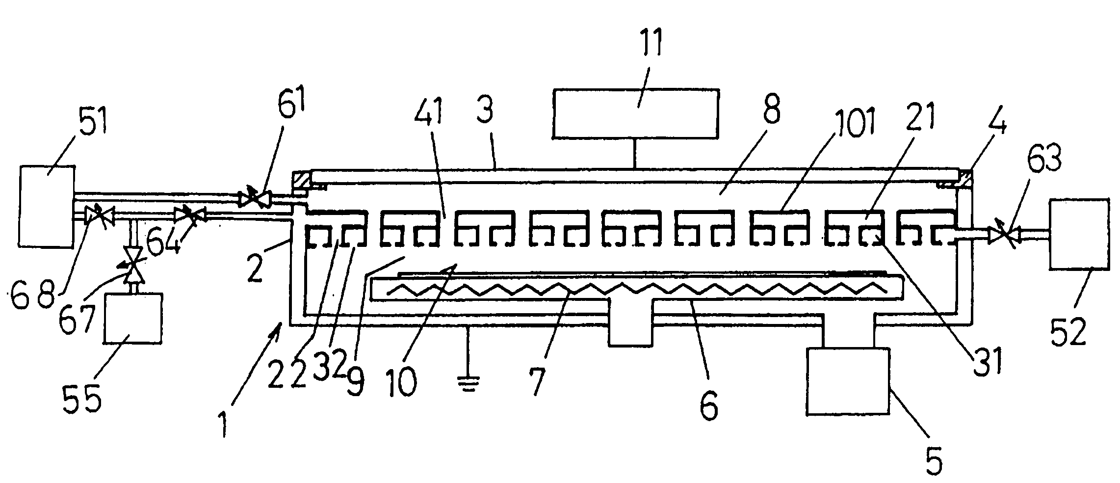
[0048]The silicon oxide film was formed on the silicon substrate by the chemical vapor deposition (CVD) under the following process conditions, using the thin film formation apparatus shown in FIG. 1.

(1) Substrate: silicon substrate

(2) Oxygen gas to be introduced into the plasma generating space:

[0049]Flow rate of 5.0×10⁻¹ (1 / mm) (1500 sccm)

(3) High frequency power: 150 W

(4) Material gas SinH2n+2 (n=1)

[0050]Flow rate of 4.0×10⁻³ (1 / mm) (20 sccm)

(5) NxOy gas (x=1, y=2) to be introduced into the second inner space:

[0051]Flow rate of 4.0×10⁻⁴ (1 / mm) (2 sccm)

(6) Oxygen gas to be introduced into the second inner space:

[0052]Flow rate of 4.0×10⁻⁴ (1 / mm) (2 sccm)

(7) Temperature of substrate (film forming temperature): 300° C.

(8) Pressure in the plasma generating space: 40 Pa

(9) Pressure in the film forming space: 40 Pa

(10) Thickness of whole thin film (film forming time): 100 nm (4 min)

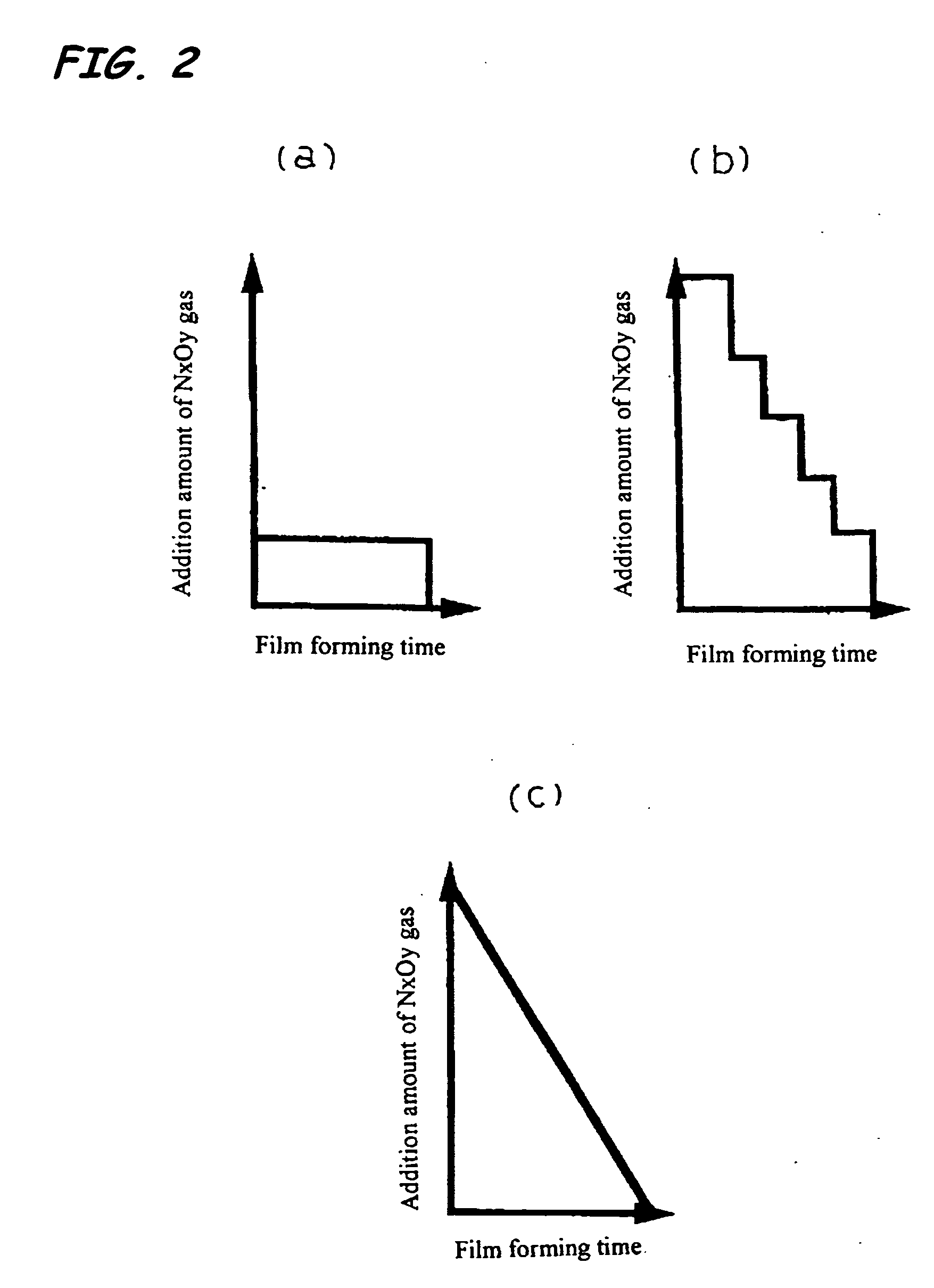
[0053]The introduction of the NxOy gas took place for about 24 seconds after the film forming process was...


PUM

PropertyMeasurementUnit
Pressureaaaaaaaaaa
Thicknessaaaaaaaaaa
flow rateaaaaaaaaaa

Abstract

A method for thin film formation that can form, at a low temperature, a good thin film having a good interfacial property between a silicon substrate and a silicon oxide film and having a low interfacial trap density is provided.The method for thin film formation comprises generating plasma within a vacuum vessel to generate an active species (radical) and forming a silicon oxide film on a silicon substrate using this active species and a material gas, wherein, in addition to the material gas, a nitrogen atom-containing gas is introduced into the vacuum vessel in its film forming space where the active species (radical) and the material gas come into contact with each other for the first time and are reacted with each other to form a silicon film on the silicon substrate, and wherein the flow rate of the nitrogen atom-containing gas during the formation of the silicon oxide film on the silicon substrate is regulated so as to be the maximum value at least at the time of the start of formation of the silicon film on the silicon substrate.

Description

BACKGROUND[0001]1. Technical Field[0002]The present invention relates to a thin film formation method in which a silicon oxide film may be formed on a silicon substrate, and more particularly to the thin film formation method that may be performed by utilizing the chemical reaction using an active species (radical).[0003]2. Background[0004]The substrate processing apparatus and method are known and used in various applications, in which substrates that are placed within the vacuum vessel of the apparatus may be processed by generating an active species (radical) by forming plasma within the vacuum vessel. For example, the substrates are processed so that the thin films can be formed on the substrates, and the surface processing is performed in order to improve the film quality of the thin films thus formed on the substrates.[0005]When the liquid crystal displays are manufactured using the polysilicon-type TFT at a low temperature, for example, the conventional substrate processing a...

Claims


Application Information

Patent Timeline
Patent Type & Authority Applications(United States)
IPC IPC(8): C23C16/00C23C16/54
CPCC23C16/401C23C16/402C23C16/452H01L21/31612H01L21/02211H01L21/02274H01L21/02164
Inventor NOGAMI, HIROSHIYUDA, KATSUHISATANABE, HIROSHI
Owner NEC CORP
Why Eureka
Try Eureka